Ingenieria
Subcategoría

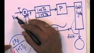
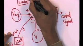
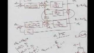
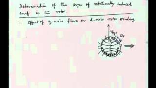
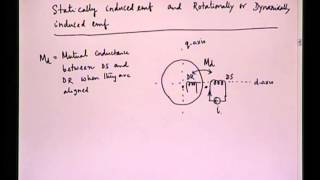
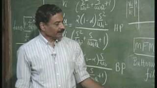
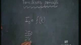
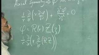
Power System Dynamics and Control by Dr. A.M. Kulkarni,Department of Electrical Engineering,IIT Bombay.For more details on NPTEL visit http://nptel.ac.in

Power System Dynamics and Control by Dr. A.M. Kulkarni,Department of Electrical Engineering,IIT Bombay.For more details on NPTEL visit http://nptel.ac.in

Power System Dynamics and Control by Dr. A.M. Kulkarni,Department of Electrical Engineering,IIT Bombay.For more details on NPTEL visit http://nptel.ac.in

Power System Dynamics and Control by Dr. A.M. Kulkarni,Department of Electrical Engineering,IIT Bombay.For more details on NPTEL visit http://nptel.ac.in

Power System Dynamics and Control by Dr. A.M. Kulkarni,Department of Electrical Engineering,IIT Bombay.For more details on NPTEL visit http://nptel.ac.in

Power System Dynamics and Control by Dr. A.M. Kulkarni,Department of Electrical Engineering,IIT Bombay.For more details on NPTEL visit http://nptel.ac.in

Power System Dynamics and Control by Dr. A.M. Kulkarni,Department of Electrical Engineering,IIT Bombay.For more details on NPTEL visit http://nptel.ac.in
Power System Dynamics and Control by Dr. A.M. Kulkarni,Department of Electrical Engineering,IIT Bombay.For more details on NPTEL visit http://nptel.ac.in

Power System Dynamics and Control by Dr. A.M. Kulkarni,Department of Electrical Engineering,IIT Bombay.For more details on NPTEL visit http://nptel.ac.in

Power System Dynamics and Control by Dr. A.M. Kulkarni,Department of Electrical Engineering,IIT Bombay.For more details on NPTEL visit http://nptel.ac.in
Power System Dynamics and Control by Dr. A.M. Kulkarni,Department of Electrical Engineering,IIT Bombay.For more details on NPTEL visit http://nptel.ac.in

Power System Dynamics and Control by Dr. A.M. Kulkarni,Department of Electrical Engineering,IIT Bombay.For more details on NPTEL visit http://nptel.ac.in
Power System Dynamics and Control by Dr. A.M. Kulkarni,Department of Electrical Engineering,IIT Bombay.For more details on NPTEL visit http://nptel.ac.in

Power System Dynamics and Control by Dr. A.M. Kulkarni,Department of Electrical Engineering,IIT Bombay.For more details on NPTEL visit http://nptel.ac.in
Power System Dynamics and Control by Dr. A.M. Kulkarni,Department of Electrical Engineering,IIT Bombay.For more details on NPTEL visit http://nptel.ac.in

Power System Dynamics and Control by Dr. A.M. Kulkarni,Department of Electrical Engineering,IIT Bombay.For more details on NPTEL visit http://nptel.ac.in

Power System Dynamics and Control by Dr. A.M. Kulkarni,Department of Electrical Engineering,IIT Bombay.For more details on NPTEL visit http://nptel.ac.in

Power System Dynamics and Control by Dr. A.M. Kulkarni,Department of Electrical Engineering,IIT Bombay.For more details on NPTEL visit http://nptel.ac.in
Power System Dynamics and Control by Dr. A.M. Kulkarni,Department of Electrical Engineering,IIT Bombay.For more details on NPTEL visit http://nptel.ac.in
Power System Dynamics and Control by Dr. A.M. Kulkarni,Department of Electrical Engineering,IIT Bombay.For more details on NPTEL visit http://nptel.ac.in

Lectures by Prof. Laxmidhar Behera, Department of Electrical Engineering, Indian Institute of Technology, Kanpur. For more details on NPTEL visit http://nptel.iitm.ac.in
Lectures by Prof. Laxmidhar Behera, Department of Electrical Engineering, Indian Institute of Technology, Kanpur. For more details on NPTEL visit http://nptel.iitm.ac.in

Lectures by Prof. Laxmidhar Behera, Department of Electrical Engineering, Indian Institute of Technology, Kanpur. For more details on NPTEL visit http://nptel.iitm.ac.in

Lectures by Prof. Laxmidhar Behera, Department of Electrical Engineering, Indian Institute of Technology, Kanpur. For more details on NPTEL visit http://nptel.iitm.ac.in

Lectures by Prof. Laxmidhar Behera, Department of Electrical Engineering, Indian Institute of Technology, Kanpur. For more details on NPTEL visit http://nptel.iitm.ac.in
Lectures by Prof. Laxmidhar Behera, Department of Electrical Engineering, Indian Institute of Technology, Kanpur. For more details on NPTEL visit http://nptel.iitm.ac.in

Lectures by Prof. Laxmidhar Behera, Department of Electrical Engineering, Indian Institute of Technology, Kanpur. For more details on NPTEL visit http://nptel.iitm.ac.in

Lectures by Prof. Laxmidhar Behera, Department of Electrical Engineering, Indian Institute of Technology, Kanpur. For more details on NPTEL visit http://nptel.iitm.ac.in
Lectures by Prof. Laxmidhar Behera, Department of Electrical Engineering, Indian Institute of Technology, Kanpur. For more details on NPTEL visit http://nptel.iitm.ac.in
Lectures by Prof. Laxmidhar Behera, Department of Electrical Engineering, Indian Institute of Technology, Kanpur. For more details on NPTEL visit http://nptel.iitm.ac.in

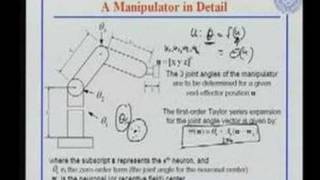
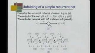
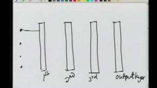
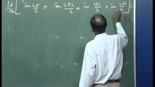
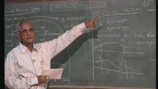
Intelligent Systems Control_M_3_L_6

Lectures by Prof. Laxmidhar Behera, Department of Electrical Engineering, Indian Institute of Technology, Kanpur. For more details on NPTEL visit http://nptel.iitm.ac.in

Lectures by Prof. Laxmidhar Behera, Department of Electrical Engineering, Indian Institute of Technology, Kanpur. For more details on NPTEL visit http://nptel.iitm.ac.in

Lectures by Prof. Laxmidhar Behera, Department of Electrical Engineering, Indian Institute of Technology, Kanpur. For more details on NPTEL visit http://nptel.iitm.ac.in

Lectures by Prof. Laxmidhar Behera, Department of Electrical Engineering, Indian Institute of Technology, Kanpur. For more details on NPTEL visit http://nptel.iitm.ac.in

Lectures by Prof. Laxmidhar Behera, Department of Electrical Engineering, Indian Institute of Technology, Kanpur. For more details on NPTEL visit http://nptel.iitm.ac.in
Lectures by Prof. Laxmidhar Behera, Department of Electrical Engineering, Indian Institute of Technology, Kanpur. For more details on NPTEL visit http://nptel.iitm.ac.in

Lectures by Prof. Laxmidhar Behera, Department of Electrical Engineering, Indian Institute of Technology, Kanpur. For more details on NPTEL visit http://nptel.iitm.ac.in

Lectures by Prof. Laxmidhar Behera, Department of Electrical Engineering, Indian Institute of Technology, Kanpur. For more details on NPTEL visit http://nptel.iitm.ac.in

Lectures by Prof. Laxmidhar Behera, Department of Electrical Engineering, Indian Institute of Technology, Kanpur. For more details on NPTEL visit http://nptel.iitm.ac.in
Lectures by Prof. Laxmidhar Behera, Department of Electrical Engineering, Indian Institute of Technology, Kanpur. For more details on NPTEL visit http://nptel.iitm.ac.in

Lectures by Prof. Laxmidhar Behera, Department of Electrical Engineering, Indian Institute of Technology, Kanpur. For more details on NPTEL visit http://nptel.iitm.ac.in
Lectures by Prof. Laxmidhar Behera, Department of Electrical Engineering, Indian Institute of Technology, Kanpur. For more details on NPTEL visit http://nptel.iitm.ac.in
Lectures by Prof. Laxmidhar Behera, Department of Electrical Engineering, Indian Institute of Technology, Kanpur.
Lectures by Prof. Laxmidhar Behera, Department of Electrical Engineering, Indian Institute of Technology, Kanpur. For more details on NPTEL visit http://nptel.iitm.ac.in
Lectures by Prof. Laxmidhar Behera, Department of Electrical Engineering, Indian Institute of Technology, Kanpur. For more details on NPTEL visit http://nptel.iitm.ac.in

Lectures by Prof. Laxmidhar Behera, Department of Electrical Engineering, Indian Institute of Technology, Kanpur. For more details on NPTEL visit http://nptel.iitm.ac.in

Lectures by Prof. Laxmidhar Behera, Department of Electrical Engineering, Indian Institute of Technology, Kanpur. For more details on NPTEL visit http://nptel.iitm.ac.in

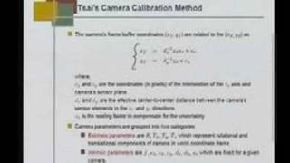
Intelligent Systems Control(M_1_L_3)Lectures by Prof. Laxmidhar Behera, Department of Electrical Engineering, Indian Institute of Technology, Kanpur. For more details on NPTEL visit http://nptel.iitm.ac.in
Lectures by Prof. Laxmidhar Behera, Department of Electrical Engineering, Indian Institute of Technology, Kanpur. For more details on NPTEL visit http://nptel.iitm.ac.in
Lectures by Prof. Laxmidhar Behera, Department of Electrical Engineering, Indian Institute of Technology, Kanpur. For more details on NPTEL visit http://nptel.iitm.ac.in

Lectures by Prof. Laxmidhar Behera, Department of Electrical Engineering, Indian Institute of Technology, Kanpur. For more details on NPTEL visit http://nptel.iitm.ac.in

Lectures by Prof.S.N.Singh Department of Electrical Engineering IIT Kanpur

Lectures by Prof.S.N.Singh Department of Electrical Engineering IIT Kanpur. For more details on NPTEL visit http://nptel.iitm.ac.in

Lectures by Prof.S.N.Singh Department of Electrical Engineering IIT Kanpur. For more details on NPTEL visit http://nptel.iitm.ac.in

Lectures by Prof.S.N.Singh Department of Electrical Engineering IIT Kanpur. For more details on NPTEL visit http://nptel.iitm.ac.in
Lectures by Prof.S.N.Singh Department of Electrical Engineering IIT Kanpur. For more details on NPTEL visit http://nptel.iitm.ac.in
Lectures by Prof.S.N.Singh Department of Electrical Engineering IIT Kanpur. For more details on NPTEL visit http://nptel.iitm.ac.in
Lectures by Prof.S.N.Singh Department of Electrical Engineering IIT Kanpur. For more details on NPTEL visit http://nptel.iitm.ac.in
Lectures by Prof.S.N.Singh Department of Electrical Engineering IIT Kanpur. For more details on NPTEL visit http://nptel.iitm.ac.in

Lectures by Prof.S.N.Singh Department of Electrical Engineering IIT Kanpur. For more details on NPTEL visit http://nptel.iitm.ac.in
Lectures by Prof.S.N.Singh Department of Electrical Engineering IIT Kanpur. For more details on NPTEL visit http://nptel.iitm.ac.in
Lectures by Prof.S.N.Singh Department of Electrical Engineering IIT Kanpur. For more details on NPTEL visit http://nptel.iitm.ac.in

Lectures by Prof.S.N.Singh Department of Electrical Engineering IIT Kanpur. For more details on NPTEL visit http://nptel.iitm.ac.in

Lectures by Prof.S.N.Singh Department of Electrical Engineering IIT Kanpur. For more details on NPTEL visit http://nptel.iitm.ac.in
Lectures by Prof.S.N.Singh Department of Electrical Engineering IIT Kanpur. For more details on NPTEL visit http://nptel.iitm.ac.in
Lectures by Prof.S.N.Singh Department of Electrical Engineering IIT Kanpur. For more details on NPTEL visit http://nptel.iitm.ac.in

Lectures by Prof.S.N.Singh Department of Electrical Engineering IIT Kanpur. For more details on NPTEL visit http://nptel.iitm.ac.in
Lectures by Prof.S.N.Singh Department of Electrical Engineering IIT Kanpur. For more details on NPTEL visit http://nptel.iitm.ac.in

Lectures by Prof.S.N.Singh Department of Electrical Engineering IIT Kanpur. For more details on NPTEL visit http://nptel.iitm.ac.in

Lectures by Prof.S.N.Singh Department of Electrical Engineering IIT Kanpur. For more details on NPTEL visit http://nptel.iitm.ac.in

Lectures by Prof.S.N.Singh Department of Electrical Engineering IIT Kanpur. For more details on NPTEL visit http://nptel.iitm.ac.in

Lectures by Prof.S.N.Singh Department of Electrical Engineering IIT Kanpur. For more details on NPTEL visit http://nptel.iitm.ac.in

Lectures by Prof.S.N.Singh Department of Electrical Engineering IIT Kanpur. For more details on NPTEL visit http://nptel.iitm.ac.in
Lectures by Prof.S.N.Singh Department of Electrical Engineering IIT Kanpur. For more details on NPTEL visit http://nptel.iitm.ac.in

Lectures by Prof.S.N.Singh Department of Electrical Engineering IIT Kanpur. For more details on NPTEL visit http://nptel.iitm.ac.in
Lectures by Prof.S.N.Singh Department of Electrical Engineering IIT Kanpur. For more details on NPTEL visit http://nptel.iitm.ac.in
Lectures by Prof.S.N.Singh Department of Electrical Engineering IIT Kanpur. For more details on NPTEL visit http://nptel.iitm.ac.in
Lectures by Prof.S.N.Singh Department of Electrical Engineering IIT Kanpur. For more details on NPTEL visit http://nptel.iitm.ac.in
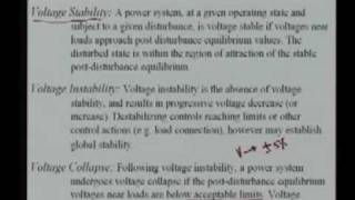
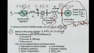
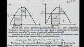
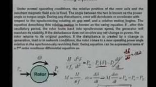
Power System Operations and Control
Module_2
Lecture_5Lectures by Prof.S.N.Singh Department of Electrical Engineering IIT Kanpur. For more details on NPTEL visit http://nptel.iitm.ac.in
Lectures by Prof.S.N.Singh Department of Electrical Engineering IIT Kanpur. For more details on NPTEL visit http://nptel.iitm.ac.in
Lectures by Prof.S.N.Singh Department of Electrical Engineering IIT Kanpur. For more details on NPTEL visit http://nptel.iitm.ac.in

Lectures by Prof.S.N.Singh Department of Electrical Engineering IIT Kanpur. For more details on NPTEL visit http://nptel.iitm.ac.in

Lectures by Prof.S.N.Singh Department of Electrical Engineering IIT Kanpur. For more details on NPTEL visit http://nptel.iitm.ac.in

Lectures by Prof.S.N.Singh Department of Electrical Engineering IIT Kanpur. For more details on NPTEL visit http://nptel.iitm.ac.in
Lectures by Prof.S.N.Singh Department of Electrical Engineering IIT Kanpur. For more details on NPTEL visit http://nptel.iitm.ac.in

Lectures by Prof.S.N.Singh Department of Electrical Engineering IIT Kanpur. For more details on NPTEL visit http://nptel.iitm.ac.in

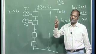
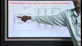
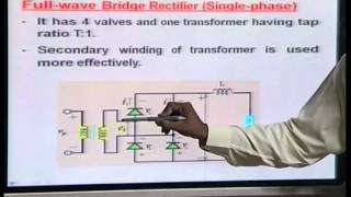
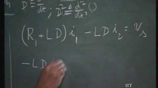
High Voltage DC Transmission by Prof.S.N.Singh,Department of Electrical Engineering,IIT Kanpur.For more details on NPTEL visit http://nptel.iitm.ac.in

High Voltage DC Transmission by Prof.S.N.Singh,Department of Electrical Engineering,IIT Kanpur.For more details on NPTEL visit http://nptel.iitm.ac.in

High Voltage DC Transmission by Prof.S.N.Singh,Department of Electrical Engineering,IIT Kanpur.For more details on NPTEL visit http://nptel.iitm.ac.in
High Voltage DC Transmission by Prof.S.N.Singh,Department of Electrical Engineering,IIT Kanpur.For more details on NPTEL visit http://nptel.iitm.ac.in
High Voltage DC Transmission by Prof.S.N.Singh,Department of Electrical Engineering,IIT Kanpur.For more details on NPTEL visit http://nptel.iitm.ac.in

High Voltage DC Transmission by Prof.S.N.Singh,Department of Electrical Engineering,IIT Kanpur.For more details on NPTEL visit http://nptel.iitm.ac.in
High Voltage DC Transmission by Prof.S.N.Singh,Department of Electrical Engineering,IIT Kanpur.For more details on NPTEL visit http://nptel.iitm.ac.in
High Voltage DC Transmission by Prof.S.N.Singh,Department of Electrical Engineering,IIT Kanpur.For more details on NPTEL visit http://nptel.iitm.ac.in
High Voltage DC Transmission by Prof.S.N.Singh,Department of Electrical Engineering,IIT Kanpur.For more details on NPTEL visit http://nptel.iitm.ac.in

High Voltage DC Transmission by Prof.S.N.Singh,Department of Electrical Engineering,IIT Kanpur.For more details on NPTEL visit http://nptel.iitm.ac.in

High Voltage DC Transmission by Prof.S.N.Singh,Department of Electrical Engineering,IIT Kanpur.For more details on NPTEL visit http://nptel.iitm.ac.in
High Voltage DC Transmission by Prof.S.N.Singh,Department of Electrical Engineering,IIT Kanpur.For more details on NPTEL visit http://nptel.iitm.ac.in
High Voltage DC Transmission by Prof.S.N.Singh,Department of Electrical Engineering,IIT Kanpur.For more details on NPTEL visit http://nptel.iitm.ac.in

High Voltage DC Transmission by Prof.S.N.Singh,Department of Electrical Engineering,IIT Kanpur.For more details on NPTEL visit http://nptel.iitm.ac.in

High Voltage DC Transmission by Prof.S.N.Singh,Department of Electrical Engineering,IIT Kanpur.For more details on NPTEL visit http://nptel.iitm.ac.in

High Voltage DC Transmission by Prof.S.N.Singh,Department of Electrical Engineering,IIT Kanpur.For more details on NPTEL visit http://nptel.iitm.ac.in

High Voltage DC Transmission by Prof.S.N.Singh,Department of Electrical Engineering,IIT Kanpur.For more details on NPTEL visit http://nptel.iitm.ac.in

High Voltage DC Transmission by Prof.S.N.Singh,Department of Electrical Engineering,IIT Kanpur.For more details on NPTEL visit http://nptel.iitm.ac.in

High Voltage DC Transmission by Prof.S.N.Singh,Department of Electrical Engineering,IIT Kanpur.For more details on NPTEL visit http://nptel.iitm.ac.in

High Voltage DC Transmission by Prof.S.N.Singh,Department of Electrical Engineering,IIT Kanpur.For more details on NPTEL visit http://nptel.iitm.ac.in

High Voltage DC Transmission by Prof.S.N.Singh,Department of Electrical Engineering,IIT Kanpur.For more details on NPTEL visit http://nptel.iitm.ac.in

High Voltage DC Transmission by Prof.S.N.Singh,Department of Electrical Engineering,IIT Kanpur.For more details on NPTEL visit http://nptel.iitm.ac.in

High Voltage DC Transmission by Prof.S.N.Singh,Department of Electrical Engineering,IIT Kanpur.For more details on NPTEL visit http://nptel.iitm.ac.in

High Voltage DC Transmission by Prof.S.N.Singh,Department of Electrical Engineering,IIT Kanpur.For more details on NPTEL visit http://nptel.iitm.ac.in

High Voltage DC Transmission by Prof.S.N.Singh,Department of Electrical Engineering,IIT Kanpur.For more details on NPTEL visit http://nptel.iitm.ac.in

High Voltage DC Transmission by Prof.S.N.Singh,Department of Electrical Engineering,IIT Kanpur.For more details on NPTEL visit http://nptel.iitm.ac.in
High Voltage DC Transmission by Prof.S.N.Singh,Department of Electrical Engineering,IIT Kanpur.For more details on NPTEL visit http://nptel.iitm.ac.in

High Voltage DC Transmission by Prof.S.N.Singh,Department of Electrical Engineering,IIT Kanpur.For more details on NPTEL visit http://nptel.iitm.ac.in

High Voltage DC Transmission by Prof.S.N.Singh,Department of Electrical Engineering,IIT Kanpur.For more details on NPTEL visit http://nptel.iitm.ac.in

High Voltage DC Transmission by Prof.S.N.Singh,Department of Electrical Engineering,IIT Kanpur.For more details on NPTEL visit http://nptel.iitm.ac.in

High Voltage DC Transmission by Prof.S.N.Singh,Department of Electrical Engineering,IIT Kanpur.For more details on NPTEL visit http://nptel.iitm.ac.in
High Voltage DC Transmission by Prof.S.N.Singh,Department of Electrical Engineering,IIT Kanpur.For more details on NPTEL visit http://nptel.iitm.ac.in
High Voltage DC Transmission by Prof.S.N.Singh,Department of Electrical Engineering,IIT Kanpur.For more details on NPTEL visit http://nptel.iitm.ac.in
High Voltage DC Transmission by Prof.S.N.Singh,Department of Electrical Engineering,IIT Kanpur.For more details on NPTEL visit http://nptel.iitm.ac.in

High Voltage DC Transmission by Prof.S.N.Singh,Department of Electrical Engineering,IIT Kanpur.For more details on NPTEL visit http://nptel.iitm.ac.in

High Voltage DC Transmission by Prof.S.N.Singh,Department of Electrical Engineering,IIT Kanpur.For more details on NPTEL visit http://nptel.iitm.ac.in

High Voltage DC Transmission by Prof.S.N.Singh,Department of Electrical Engineering,IIT Kanpur.For more details on NPTEL visit http://nptel.iitm.ac.in
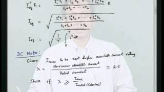
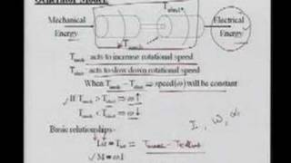
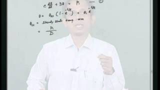
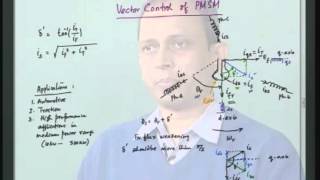
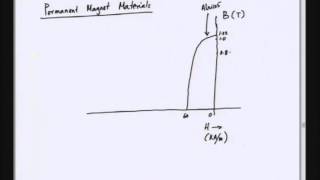
Advanced Electric Drives by Dr. S.P. Das, Department of Electrical Engineering,IIT Kanpur.For more details on NPTEL visit http://nptel.iitm.ac.in
Advanced Electric Drives by Dr. S.P. Das, Department of Electrical Engineering,IIT Kanpur.For more details on NPTEL visit http://nptel.iitm.ac.in

Advanced Electric Drives by Dr. S.P. Das, Department of Electrical Engineering,IIT Kanpur.For more details on NPTEL visit http://nptel.iitm.ac.in

Advanced Electric Drives by Dr. S.P. Das, Department of Electrical Engineering,IIT Kanpur.For more details on NPTEL visit http://nptel.iitm.ac.in

Advanced Electric Drives by Dr. S.P. Das, Department of Electrical Engineering,IIT Kanpur.For more details on NPTEL visit http://nptel.iitm.ac.in

Advanced Electric Drives by Dr. S.P. Das, Department of Electrical Engineering,IIT Kanpur.For more details on NPTEL visit http://nptel.iitm.ac.in
Advanced Electric Drives by Dr. S.P. Das, Department of Electrical Engineering,IIT Kanpur.For more details on NPTEL visit http://nptel.iitm.ac.in
Advanced Electric Drives by Dr. S.P. Das, Department of Electrical Engineering,IIT Kanpur.For more details on NPTEL visit http://nptel.iitm.ac.in
Advanced Electric Drives by Dr. S.P. Das, Department of Electrical Engineering,IIT Kanpur.For more details on NPTEL visit http://nptel.iitm.ac.in

Advanced Electric Drives by Dr. S.P. Das, Department of Electrical Engineering,IIT Kanpur.For more details on NPTEL visit http://nptel.iitm.ac.in

Advanced Electric Drives by Dr. S.P. Das, Department of Electrical Engineering,IIT Kanpur.For more details on NPTEL visit http://nptel.iitm.ac.in
Advanced Electric Drives by Dr. S.P. Das, Department of Electrical Engineering,IIT Kanpur.For more details on NPTEL visit http://nptel.iitm.ac.in

Advanced Electric Drives by Dr. S.P. Das, Department of Electrical Engineering,IIT Kanpur.For more details on NPTEL visit http://nptel.iitm.ac.in
Advanced Electric Drives by Dr. S.P. Das, Department of Electrical Engineering,IIT Kanpur.For more details on NPTEL visit http://nptel.iitm.ac.in
Advanced Electric Drives by Dr. S.P. Das, Department of Electrical Engineering,IIT Kanpur.For more details on NPTEL visit http://nptel.iitm.ac.in
Advanced Electric Drives by Dr. S.P. Das, Department of Electrical Engineering,IIT Kanpur.For more details on NPTEL visit http://nptel.iitm.ac.in
Advanced Electric Drives by Dr. S.P. Das, Department of Electrical Engineering,IIT Kanpur.For more details on NPTEL visit http://nptel.iitm.ac.in

Advanced Electric Drives by Dr. S.P. Das, Department of Electrical Engineering,IIT Kanpur.For more details on NPTEL visit http://nptel.iitm.ac.in
Advanced Electric Drives by Dr. S.P. Das, Department of Electrical Engineering,IIT Kanpur.For more details on NPTEL visit http://nptel.iitm.ac.in
Advanced Electric Drives by Dr. S.P. Das, Department of Electrical Engineering,IIT Kanpur.For more details on NPTEL visit http://nptel.iitm.ac.in

Advanced Electric Drives by Dr. S.P. Das, Department of Electrical Engineering,IIT Kanpur.For more details on NPTEL visit http://nptel.iitm.ac.in
Advanced Electric Drives by Dr. S.P. Das, Department of Electrical Engineering,IIT Kanpur.For more details on NPTEL visit http://nptel.iitm.ac.in

Advanced Electric Drives by Dr. S.P. Das, Department of Electrical Engineering,IIT Kanpur.For more details on NPTEL visit http://nptel.iitm.ac.in

Advanced Electric Drives by Dr. S.P. Das, Department of Electrical Engineering,IIT Kanpur.For more details on NPTEL visit http://nptel.iitm.ac.in

Advanced Electric Drives by Dr. S.P. Das, Department of Electrical Engineering,IIT Kanpur.For more details on NPTEL visit http://nptel.iitm.ac.in

Advanced Electric Drives by Dr. S.P. Das, Department of Electrical Engineering,IIT Kanpur.For more details on NPTEL visit http://nptel.iitm.ac.in

Advanced Electric Drives by Dr. S.P. Das, Department of Electrical Engineering,IIT Kanpur.For more details on NPTEL visit http://nptel.iitm.ac.in
Advanced Electric Drives by Dr. S.P. Das, Department of Electrical Engineering,IIT Kanpur.For more details on NPTEL visit http://nptel.iitm.ac.in

Advanced Electric Drives by Dr. S.P. Das, Department of Electrical Engineering,IIT Kanpur.For more details on NPTEL visit http://nptel.iitm.ac.in

Advanced Electric Drives by Dr. S.P. Das, Department of Electrical Engineering,IIT Kanpur.For more details on NPTEL visit http://nptel.iitm.ac.in
Advanced Electric Drives by Dr. S.P. Das, Department of Electrical Engineering,IIT Kanpur.For more details on NPTEL visit http://nptel.iitm.ac.in
Advanced Electric Drives by Dr. S.P. Das, Department of Electrical Engineering,IIT Kanpur.For more details on NPTEL visit http://nptel.iitm.ac.in

Lecture Series on Computer Organization by Prof.S. Raman, Department of Computer Science and Engineering, IIT Madras. For More details on NPTEL visit http://nptel.iitm.ac.in

Lecture series on Digital Circuits & Systems by Prof. S. Srinivasan,
Department of Electrical Engineering, IIT Madras
For more details on NPTEL visit http://nptel.iitm.ac.in
Lecture series on Digital Circuits & Systems by Prof. S. Srinivasan,
Department of Electrical Engineering, IIT Madras
For more details on NPTEL visit http://nptel.iitm.ac.in

Lecture series on Digital Circuits & Systems by Prof. S. Srinivasan,
Department of Electrical Engineering, IIT Madras
For more details on NPTEL visit http://nptel.iitm.ac.in

Lecture series on Digital Circuits & Systems by Prof. S. Srinivasan,
Department of Electrical Engineering, IIT Madras
For more details on NPTEL visit http://nptel.iitm.ac.in
Lecture series on Digital Circuits & Systems by Prof. S. Srinivasan,
Department of Electrical Engineering, IIT Madras
For more details on NPTEL visit http://nptel.iitm.ac.in

Lecture series on Digital Circuits & Systems by Prof. S. Srinivasan,
Department of Electrical Engineering, IIT Madras
For more details on NPTEL visit http://nptel.iitm.ac.in
Lecture series on Digital Circuits & Systems by Prof. S. Srinivasan,
Department of Electrical Engineering, IIT Madras
For more details on NPTEL visit http://nptel.iitm.ac.in

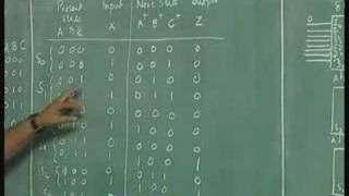
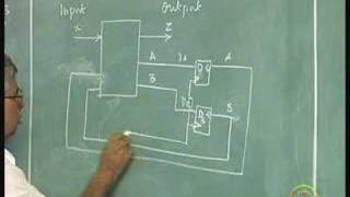
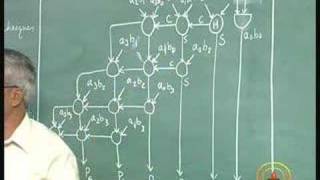
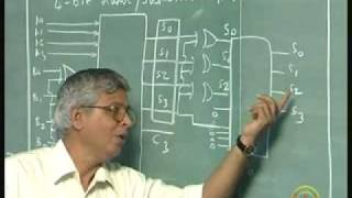
Digital Circuit system

Lecture series on Digital Circuits & Systems by Prof. S. Srinivasan,
Department of Electrical Engineering, IIT Madras
For more details on NPTEL visit http://nptel.iitm.ac.in

Lecture series on Digital Circuits & Systems by Prof. S. Srinivasan,
Department of Electrical Engineering, IIT Madras
For more details on NPTEL visit http://nptel.iitm.ac.in

Lecture series on Digital Circuits & Systems by Prof.S.Srinivasan, Department of Electrical Engineering, IIT Madras.For more details on NPTEL visit http://nptel.iitm.ac.in

Lecture series on Digital Circuits & Systems by Prof. S. Srinivasan,
Department of Electrical Engineering, IIT Madras
For more details on NPTEL visit http://nptel.iitm.ac.in

Lecture series on Digital Circuits & Systems by Prof. S. Srinivasan,
Department of Electrical Engineering, IIT Madras
For more details on NPTEL visit http://nptel.iitm.ac.in

Lecture series on Digital Circuits & Systems by Prof. S. Srinivasan,
Department of Electrical Engineering, IIT Madras
For more details on NPTEL visit http://nptel.iitm.ac.in

Lecture series on Digital Circuits & Systems by Prof. S. Srinivasan,
Department of Electrical Engineering, IIT Madras
For more details on NPTEL visit http://nptel.iitm.ac.in

Lecture series on Digital Circuits & Systems by Prof. S. Srinivasan,
Department of Electrical Engineering, IIT Madras
For more details on NPTEL visit http://nptel.iitm.ac.in

Lecture series on Digital Circuits & Systems by Prof. S. Srinivasan,
Department of Electrical Engineering, IIT Madras
For more details on NPTEL visit http://nptel.iitm.ac.in
Lecture series on Digital Circuits & Systems by Prof. S. Srinivasan,
Department of Electrical Engineering, IIT Madras
For more details on NPTEL visit http://nptel.iitm.ac.in

Lecture series on Digital Circuits & Systems by Prof. S. Srinivasan,
Department of Electrical Engineering, IIT Madras
For more details on NPTEL visit http://nptel.iitm.ac.in

Lecture series on Digital Circuits & Systems by Prof. S. Srinivasan,
Department of Electrical Engineering, IIT Madras
For more details on NPTEL visit http://nptel.iitm.ac.in

Lecture series on Digital Circuits & Systems by Prof. S. Srinivasan,
Department of Electrical Engineering, IIT Madras
For more details on NPTEL visit http://nptel.iitm.ac.in
Lecture series on Digital Circuits & Systems by Prof. S. Srinivasan,
Department of Electrical Engineering, IIT Madras
For more details on NPTEL visit http://nptel.iitm.ac.in

Lecture series on Digital Circuits & Systems by Prof. S. Srinivasan,
Department of Electrical Engineering, IIT Madras
For more details on NPTEL visit http://nptel.iitm.ac.in

Lecture series on Digital Circuits & Systems by Prof. S. Srinivasan,
Department of Electrical Engineering, IIT Madras
For more details on NPTEL visit http://nptel.ac.in

Lecture series on Digital Circuits & Systems by Prof. S. Srinivasan,
Department of Electrical Engineering, IIT Madras
For more details on NPTEL visit http://nptel.ac.in
Lecture series on Digital Circuits & Systems by Prof. S. Srinivasan,
Department of Electrical Engineering, IIT Madras
For more details on NPTEL visit http://nptel.iitm.ac.in
Lecture series on Digital Circuits & Systems by Prof. S. Srinivasan,
Department of Electrical Engineering, IIT Madras
For more details on NPTEL visit http://nptel.iitm.ac.in

Lecture series on Digital Circuits & Systems by Prof. S. Srinivasan,
Department of Electrical Engineering, IIT Madras
For more details on NPTEL visit http://nptel.iitm.ac.in

Lecture series on Digital Circuits & Systems by Prof. S. Srinivasan,
Department of Electrical Engineering, IIT Madras
For more details on NPTEL visit http://nptel.iitm.ac.in

Lecture series on Digital Circuits & Systems by Prof. S. Srinivasan,
Department of Electrical Engineering, IIT Madras
For more details on NPTEL visit http://nptel.iitm.ac.in

Lecture series on Digital Circuits & Systems by Prof. S. Srinivasan,
Department of Electrical Engineering, IIT Madras
For more details on NPTEL visit http://nptel.iitm.ac.in

Lecture series on Digital Circuits & Systems by Prof. S. Srinivasan,
Department of Electrical Engineering, IIT Madras
For more details on NPTEL visit http://nptel.iitm.ac.in

Lecture series on Digital Circuits & Systems by Prof. S. Srinivasan,
Department of Electrical Engineering, IIT Madras
For more details on NPTEL visit http://nptel.iitm.ac.in

Lecture series on Digital Circuits & Systems by Prof. S. Srinivasan,
Department of Electrical Engineering, IIT Madras
For more details on NPTEL visit http://nptel.iitm.ac.in

Lecture series on Digital Circuits & Systems by Prof. S. Srinivasan,
Department of Electrical Engineering, IIT Madras
For more details on NPTEL visit http://nptel.iitm.ac.in

Lecture series on Digital Circuits & Systems by Prof. S. Srinivasan,
Department of Electrical Engineering, IIT Madras
For more details on NPTEL visit http://nptel.iitm.ac.in

Lecture series on Digital Circuits & Systems by Prof. S. Srinivasan,
Department of Electrical Engineering, IIT Madras
For more details on NPTEL visit http://nptel.iitm.ac.in

Lecture series on Digital Circuits & Systems by Prof. S. Srinivasan,
Department of Electrical Engineering, IIT Madras
For more details on NPTEL visit http://nptel.iitm.ac.in

Lecture series on Digital Circuits & Systems by Prof. S. Srinivasan,
Department of Electrical Engineering, IIT Madras
For more details on NPTEL visit http://nptel.iitm.ac.in

Lecture series on Digital Circuits & Systems by Prof.S.Srinivasan, Department of Electrical Engineering, IIT Madras.For more details on NPTEL visit http://nptel.ac.in

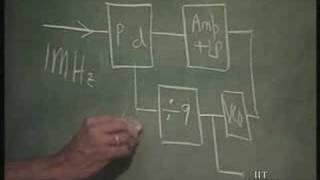
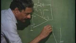
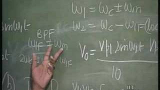
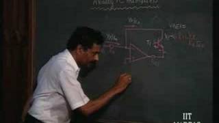
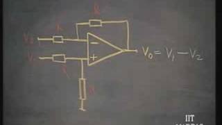
Lecture Series on Electronics for Analog Signal Processing I by Prof. K. Radhakrishna Rao, Department of Electrical Engineering, IIT Madras. For more details on NPTEL visit http://nptel.iitm.ac.in
Lecture Series on Electronics for Analog Signal Processing I by Prof. K. Radhakrishna Rao, Department of Electrical Engineering, IIT Madras. For more details on NPTEL visit http://nptel.iitm.ac.in

Lecture Series on Electronics for Analog Signal Processing I by Prof. K. Radhakrishna Rao, Department of Electrical Engineering, IIT Madras. For more details on NPTEL visit http://nptel.iitm.ac.in

Lecture Series on Electronics for Analog Signal Processing I by Prof. K. Radhakrishna Rao, Department of Electrical Engineering, IIT Madras. For more details on NPTEL visit http://nptel.iitm.ac.in

Lecture Series on Electronics for Analog Signal Processing I by Prof. K. Radhakrishna Rao, Department of Electrical Engineering, IIT Madras. For more details on NPTEL visit http://nptel.iitm.ac.in
Lecture Series on Electronics for Analog Signal Processing I by Prof. K. Radhakrishna Rao, Department of Electrical Engineering, IIT Madras. For more details on NPTEL visit http://nptel.iitm.ac.in

Lecture Series on Electronics for Analog Signal Processing I by Prof. K. Radhakrishna Rao, Department of Electrical Engineering, IIT Madras. For more details on NPTEL visit http://nptel.iitm.ac.in

Lecture Series on Electronics for Analog Signal Processing I by Prof. K. Radhakrishna Rao, Department of Electrical Engineering, IIT Madras. For more details on NPTEL visit http://nptel.iitm.ac.in
Lecture Series on Electronics For Analog Signal Processing I by Prof.K.Radhakrishna Rao, Department of Electrical Engineering,IIT Madras. For more details on NPTEL visit http://nptel.iitm.ac.in

Lecture Series on Electronics For Analog Signal Processing I by Prof.K.Radhakrishna Rao, Department of Electrical Engineering,IIT Madras. For more details on NPTEL visit http://nptel.iitm.ac.in
Lecture Series on Electronics For Analog Signal Processing by Prof.K.Radhakrishna Rao, Department of Electrical Engineering,IIT Madras. For more details on NPTEL visit http://nptel.iitm.ac.in
Lecture Series on Electronics For Analog Signal Processing I by Prof.K.Radhakrishna Rao, Department of Electrical Engineering,IIT Madras. For more details on NPTEL visit http://nptel.iitm.ac.in
Lecture Series on Electronics For Analog Signal Processing I by Prof.K.Radhakrishna Rao, Department of Electrical Engineering,IIT Madras. For more details on NPTEL visit http://nptel.iitm.ac.in
Lecture Series on Electronics For Analog Signal Processing I by Prof.K.Radhakrishna Rao, Department of Electrical Engineering,IIT Madras. For more details on NPTEL visit http://nptel.iitm.ac.in

Lecture Series on Electronics For Analog Signal Processing I by Prof.K.Radhakrishna Rao, Department of Electrical Engineering,IIT Madras. For more details on NPTEL visit http://nptel.iitm.ac.in
Lecture Series on Electronics For Analog Signal Processing I by Prof.K.Radhakrishna Rao, Department of Electrical Engineering,IIT Madras. For more details on NPTEL visit http://nptel.iitm.ac.in
Lecture Series on Electronics For Analog Signal Processing I by Prof.K.Radhakrishna Rao, Department of Electrical Engineering,IIT Madras. For more details on NPTEL visit http://nptel.iitm.ac.in

Lecture Series on Electronics For Analog Signal Processing I by Prof.K.Radhakrishna Rao, Department of Electrical Engineering,IIT Madras. For more details on NPTEL visit http://nptel.iitm.ac.in
Lecture Series on Electronics For Analog Signal Processing I by Prof.K.Radhakrishna Rao, Department of Electrical Engineering,IIT Madras. For more details on NPTEL visit http://nptel.iitm.ac.in

Lecture Series on Electronics For Analog Signal Processing I by Prof.K.Radhakrishna Rao, Department of Electrical Engineering,IIT Madras. For more details on NPTEL visit http://nptel.iitm.ac.in

Lecture Series on Electronics For Analog Signal Processing I by Prof.K.Radhakrishna Rao, Department of Electrical Engineering,IIT Madras. For more details on NPTEL visit http://nptel.iitm.ac.in

Lecture Series on Electronics For Analog Signal Processing I by Prof.K.Radhakrishna Rao, Department of Electrical Engineering,IIT Madras. For more details on NPTEL visit http://nptel.iitm.ac.in

Lecture Series on Electronics For Analog Signal Processing I by Prof.K.Radhakrishna Rao, Department of Electrical Engineering,IIT Madras. For more details on NPTEL visit http://nptel.iitm.ac.in

Lecture Series on Electronics For Analog Signal Processing I by Prof.K.Radhakrishna Rao, Department of Electrical Engineering,IIT Madras. For more details on NPTEL visit http://nptel.iitm.ac.in
Lecture Series on Electronics For Analog Signal Processing I by Prof.K.Radhakrishna Rao, Department of Electrical Engineering,IIT Madras. For more details on NPTEL visit http://nptel.iitm.ac.in

Lecture Series on Electronics For Analog Signal Processing I by Prof.K.Radhakrishna Rao, Department of Electrical Engineering,IIT Madras. For more details on NPTEL visit http://nptel.iitm.ac.in
Lecture Series on Electronics For Analog Signal Processing I by Prof.K.Radhakrishna Rao, Department of Electrical Engineering,IIT Madras. For more details on NPTEL visit http://nptel.iitm.ac.in

Lecture Series on Electronics For Analog Signal Processing I by Prof.K.Radhakrishna Rao, Department of Electrical Engineering,IIT Madras. For more details on NPTEL visit http://nptel.iitm.ac.in

Lecture Series on Electronics For Analog Signal Processing I by Prof.K.Radhakrishna Rao, Department of Electrical Engineering,IIT Madras. For more details on NPTEL visit http://nptel.iitm.ac.in

Lecture Series on Electronics For Analog Signal Processing I by Prof.K.Radhakrishna Rao, Department of Electrical Engineering,IIT Madras. For more details on NPTEL visit http://nptel.iitm.ac.in
Lecture Series on Electronics For Analog Signal Processing I by Prof.K.Radhakrishna Rao, Department of Electrical Engineering,IIT Madras. For more details on NPTEL visit http://nptel.iitm.ac.in

Lecture Series on Electronics For Analog Signal Processing I by Prof.K.Radhakrishna Rao, Department of Electrical Engineering,IIT Madras. For more details on NPTEL visit http://nptel.iitm.ac.in

Lecture Series on Electronics For Analog Signal Processing I by Prof.K.Radhakrishna Rao, Department of Electrical Engineering,IIT Madras. For more details on NPTEL visit http://nptel.iitm.ac.in

Lecture Series on Electronics For Analog Signal Processing I by Prof.K.Radhakrishna Rao, Department of Electrical Engineering,IIT Madras. For more details on NPTEL visit http://nptel.iitm.ac.in

Lecture Series on Electronics For Analog Signal Processing I by Prof.K.Radhakrishna Rao, Department of Electrical Engineering,IIT Madras. For more details on NPTEL visit http://nptel.iitm.ac.in

Lecture Series on Electronics For Analog Signal Processing I by Prof.K.Radhakrishna Rao, Department of Electrical Engineering,IIT Madras. For more details on NPTEL visit http://nptel.iitm.ac.in

Lecture Series on Electronics For Analog Signal Processing I by Prof.K.Radhakrishna Rao, Department of Electrical Engineering,IIT Madras. For more details on NPTEL visit http://nptel.iitm.ac.in
Lecture Series on Electronics For Analog Signal Processing I by Prof.K.Radhakrishna Rao, Department of Electrical Engineering,IIT Madras. For more details on NPTEL visit http://nptel.iitm.ac.in
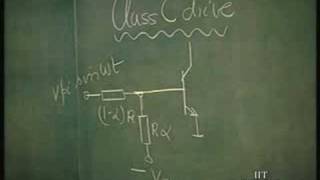
Lecture Series on Electronics For Analog Signal Processing part-II by Prof.K.Radhakrishna Rao, Department of Electrical Engineering,IIT Madras. For more details on NPTEL visit http://nptel.iitm.ac.in
Lecture Series on Electronics For Analog Signal Processing part-II by Prof.K.Radhakrishna Rao, Department of Electrical Engineering,IIT Madras. For more details on NPTEL visit http://nptel.iitm.ac.in

Lecture Series on Electronics For Analog Signal Processing part-II by Prof.K.Radhakrishna Rao, Department of Electrical Engineering,IIT Madras. For more details on NPTEL visit http://nptel.iitm.ac.in

Lecture Series on Electronics For Analog Signal Processing part-II by Prof.K.Radhakrishna Rao, Department of Electrical Engineering,IIT Madras. For more details on NPTEL visit http://nptel.iitm.ac.in

Lecture Series on Electronics For Analog Signal Processing part-II by Prof.K.Radhakrishna Rao, Department of Electrical Engineering,IIT Madras. For more details on NPTEL visit http://nptel.iitm.ac.in
Lecture Series on Electronics For Analog Signal Processing part-II by Prof.K.Radhakrishna Rao, Department of Electrical Engineering,IIT Madras. For more details on NPTEL visit http://nptel.iitm.ac.in

Lecture Series on Electronics For Analog Signal Processing part-II by Prof.K.Radhakrishna Rao, Department of Electrical Engineering,IIT Madras. For more details on NPTEL visit http://nptel.iitm.ac.in
Lecture Series on Electronics For Analog Signal Processing part-II by Prof.K.Radhakrishna Rao, Department of Electrical Engineering,IIT Madras. For more details on NPTEL visit http://nptel.iitm.ac.in

Lecture Series on Electronics For Analog Signal Processing part-II by Prof.K.Radhakrishna Rao, Department of Electrical Engineering,IIT Madras. For more details on NPTEL visit http://nptel.iitm.ac.in

Lecture Series on Electronics For Analog Signal Processing part-II by Prof.K.Radhakrishna Rao, Department of Electrical Engineering,IIT Madras. For more details on NPTEL visit http://nptel.iitm.ac.in

Lecture Series on Electronics For Analog Signal Processing part-II by Prof.K.Radhakrishna Rao, Department of Electrical Engineering,IIT Madras. For more details on NPTEL visit http://nptel.iitm.ac.in

Lecture Series on Electronics For Analog Signal Processing part-II by Prof.K.Radhakrishna Rao, Department of Electrical Engineering,IIT Madras. For more details on NPTEL visit http://nptel.iitm.ac.in

Lecture Series on Electronics For Analog Signal Processing part-II by Prof.K.Radhakrishna Rao, Department of Electrical Engineering,IIT Madras. For more details on NPTEL visit http://nptel.iitm.ac.in

Lecture Series on Electronics For Analog Signal Processing part-II by Prof.K.Radhakrishna Rao, Department of Electrical Engineering,IIT Madras. For more details on NPTEL visit http://nptel.iitm.ac.in

Lecture Series on Electronics For Analog Signal Processing part-II by Prof.K.Radhakrishna Rao, Department of Electrical Engineering,IIT Madras. For more details on NPTEL visit http://nptel.iitm.ac.in
Lecture Series on Electronics For Analog Signal Processing part-II by Prof.K.Radhakrishna Rao, Department of Electrical Engineering,IIT Madras. For more details on NPTEL visit http://nptel.iitm.ac.in

Lecture Series on Electronics For Analog Signal Processing part-II by Prof.K.Radhakrishna Rao, Department of Electrical Engineering,IIT Madras. For more details on NPTEL visit http://nptel.iitm.ac.in

Lecture Series on Electronics For Analog Signal Processing part-II by Prof.K.Radhakrishna Rao, Department of Electrical Engineering,IIT Madras. For more details on NPTEL visit http://nptel.iitm.ac.in

Lecture Series on Electronics For Analog Signal Processing part-II by Prof.K.Radhakrishna Rao, Department of Electrical Engineering,IIT Madras. For more details on NPTEL visit http://nptel.iitm.ac.in

Lecture Series on Electronics For Analog Signal Processing part-II by Prof.K.Radhakrishna Rao, Department of Electrical Engineering,IIT Madras. For more details on NPTEL visit http://nptel.iitm.ac.in

Lecture Series on Electronics For Analog Signal Processing part-II by Prof.K.Radhakrishna Rao, Department of Electrical Engineering,IIT Madras. For more details on NPTEL visit http://nptel.iitm.ac.in
Lecture Series on Electronics For Analog Signal Processing part-II by Prof.K.Radhakrishna Rao, Department of Electrical Engineering,IIT Madras. For more details on NPTEL visit http://nptel.iitm.ac.in
Lecture Series on Electronics For Analog Signal Processing part-II by Prof.K.Radhakrishna Rao, Department of Electrical Engineering,IIT Madras. For more details on NPTEL visit http://nptel.iitm.ac.in
Lecture Series on Electronics For Analog Signal Processing part-II by Prof.K.Radhakrishna Rao, Department of Electrical Engineering,IIT Madras. For more details on NPTEL visit http://nptel.iitm.ac.in

Lecture Series on Electronics For Analog Signal Processing part-II by Prof.K.Radhakrishna Rao, Department of Electrical Engineering,IIT Madras. For more details on NPTEL visit http://nptel.iitm.ac.in

Lecture Series on Electronics For Analog Signal Processing part-II by Prof.K.Radhakrishna Rao, Department of Electrical Engineering,IIT Madras. For more details on NPTEL visit http://nptel.iitm.ac.in
Lecture Series on Electronics For Analog Signal Processing part-II by Prof.K.Radhakrishna Rao, Department of Electrical Engineering,IIT Madras. For more details on NPTEL visit http://nptel.iitm.ac.in
Lecture Series on Electronics For Analog Signal Processing part-II by Prof.K.Radhakrishna Rao, Department of Electrical Engineering,IIT Madras. For more details on NPTEL visit http://nptel.iitm.ac.in

Lecture Series on Electronics For Analog Signal Processing part-II by Prof.K.Radhakrishna Rao, Department of Electrical Engineering,IIT Madras. For more details on NPTEL visit http://nptel.iitm.ac.in

Lecture Series on Electronics For Analog Signal Processing part-II by Prof.K.Radhakrishna Rao, Department of Electrical Engineering,IIT Madras. For more details on NPTEL visit http://nptel.iitm.ac.in

Lecture Series on Electronics For Analog Signal Processing part-II by Prof.K.Radhakrishna Rao, Department of Electrical Engineering,IIT Madras. For more details on NPTEL visit http://nptel.iitm.ac.in

Lecture Series on Electronics For Analog Signal Processing part-II by Prof.K.Radhakrishna Rao, Department of Electrical Engineering,IIT Madras. For more details on NPTEL visit http://nptel.iitm.ac.in

Lecture Series on Electronics For Analog Signal Processing part-II by Prof.K.Radhakrishna Rao, Department of Electrical Engineering,IIT Madras. For more details on NPTEL visit http://nptel.iitm.ac.in

Lecture Series on Electronics For Analog Signal Processing part-II by Prof.K.Radhakrishna Rao, Department of Electrical Engineering,IIT Madras. For more details on NPTEL visit http://nptel.iitm.ac.in

Lecture Series on Electronics For Analog Signal Processing part-II by Prof.K.Radhakrishna Rao, Department of Electrical Engineering,IIT Madras. For more details on NPTEL visit http://nptel.iitm.ac.in

Lecture Series on Electronics For Analog Signal Processing part-II by Prof.K.Radhakrishna Rao, Department of Electrical Engineering,IIT Madras. For more details on NPTEL visit http://nptel.iitm.ac.in

Lecture Series on Electronics For Analog Signal Processing part-II by Prof.K.Radhakrishna Rao, Department of Electrical Engineering,IIT Madras. For more details on NPTEL visit http://nptel.iitm.ac.in
Lecture Series on Electronics For Analog Signal Processing part-II by Prof.K.Radhakrishna Rao, Department of Electrical Engineering,IIT Madras. For more details on NPTEL visit http://nptel.iitm.ac.in

Lecture Series on Electronics For Analog Signal Processing part-II by Prof.K.Radhakrishna Rao, Department of Electrical Engineering,IIT Madras. For more details on NPTEL visit http://nptel.iitm.ac.in

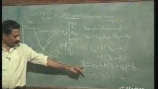
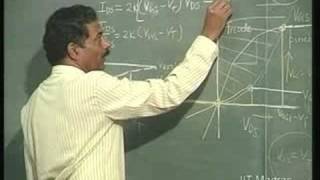
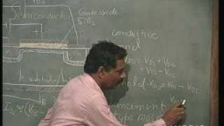
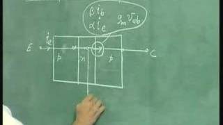
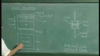
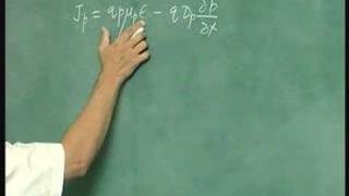
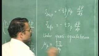
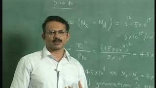
Solid State Devises

Solid State Devices
Solid State Devices
Solid State Devices

Solid State Devices

Solid State Devices

Solid State Devices

Solid State Devices

Solid State Devices

Solid State Devices
Solid State Devices
Solid State Devices
Solid State Devices

Solid State Devices
Solid State Devices

Solid State Devices
Solid State Devices
Solid State Devices
Solid State Devices
Solid State Devices

Solid State Devices

Solid State Devices

Solid State Devices
Solid State Devices

Solid State Devices
Solid State Devices

Solid State Devices

Solid State Devices

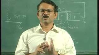
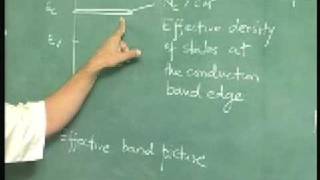
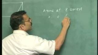
Lecture series on Solid State Devices by Prof S.Karmalkar, Dept of Electrical Engineering IIT Madras. For more details on NPTEL visit http://nptel.iitm.ac.in
Solid State Devices

Lecture Series on Solid State Devices by Dr.S.Karmalkar, Department of Electrical Engineering, IIT Madras. For more details on NPTEL visit http://nptel.iitm.ac.in
Lecture Series on Solid State Devices by Dr.S.Karmalkar, Department of Electrical Engineering, IIT Madras. For more details on NPTEL visit http://nptel.iitm.ac.in

Lecture Series on Solid State Devices by Dr.S.Karmalkar, Department of Electrical Engineering, IIT Madras. For more details on NPTEL visit http://nptel.iitm.ac.in

Lecture Series on Solid State Devices by Dr.S.Karmalkar, Department of Electrical Engineering, IIT Madras. For more details on NPTEL visit http://nptel.iitm.ac.in
Lecture Series on Solid State Devices by Dr.S.Karmalkar, Department of Electrical Engineering, IIT Madras. For more details on NPTEL visit http://nptel.iitm.ac.in

Lecture Series on Solid State Devices by Dr.S.Karmalkar, Department of Electrical Engineering, IIT Madras. For more details on NPTEL visit http://nptel.iitm.ac.in

Lecture Series on Solid State Devices by Dr.S.Karmalkar, Department of Electrical Engineering, IIT Madras. For more details on NPTEL visit http://nptel.iitm.ac.in

Lecture Series on Solid State Devices by Dr.S.Karmalkar, Department of Electrical Engineering, IIT Madras. For more details on NPTEL visit http://nptel.iitm.ac.in
Lecture Series on Solid State Devices by Dr.S.Karmalkar, Department of Electrical Engineering, IIT Madras. For more details on NPTEL visit http://nptel.iitm.ac.in
Lecture Series on Solid State Devices by Dr.S.Karmalkar, Department of Electrical Engineering, IIT Madras. For more details on NPTEL visit http://nptel.iitm.ac.in

Lecture Series on Solid State Devices by Dr.S.Karmalkar, Department of Electrical Engineering, IIT Madras. For more details on NPTEL visit http://nptel.iitm.ac.in

Lecture Series on Solid State Devices by Dr.S.Karmalkar, Department of Electrical Engineering, IIT Madras. For more details on NPTEL visit http://nptel.iitm.ac.in

VLSI
VLSI

VLSI

VLSI

VLSI

Lecture Series on VLSI Design by Dr.Nandita Dasgupta, Department of Electrical Engineering, IIT Madras. For more details on NPTEL visit http://nptel.iitm.ac.in
Lecture Series on VLSI Design by Dr.Nandita Dasgupta, Department of Electrical Engineering, IIT Madras. For more details on NPTEL visit http://nptel.iitm.ac.in
Lecture Series on VLSI Design by Dr.Nandita Dasgupta, Department of Electrical Engineering, IIT Madras. For more details on NPTEL visit http://nptel.iitm.ac.in

Lecture Series on VLSI Design by Dr.Nandita Dasgupta, Department of Electrical Engineering, IIT Madras. For more details on NPTEL visit http://nptel.iitm.ac.in

Lecture Series on VLSI Design by Dr.Nandita Dasgupta, Department of Electrical Engineering, IIT Madras. For more details on NPTEL visit http://nptel.iitm.ac.in

Lecture Series on VLSI Design by Dr.Nandita Dasgupta, Department of Electrical Engineering, IIT Madras. For more details on NPTEL visit http://nptel.iitm.ac.in

Lecture Series on VLSI Design by Dr.Nandita Dasgupta, Department of Electrical Engineering, IIT Madras. For more details on NPTEL visit http://nptel.iitm.ac.in

Lecture Series on VLSI Design by Dr.Nandita Dasgupta, Department of Electrical Engineering, IIT Madras. For more details on NPTEL visit http://nptel.iitm.ac.in

Lecture Series on VLSI Design by Dr.Nandita Dasgupta, Department of Electrical Engineering, IIT Madras. For more details on NPTEL visit http://nptel.iitm.ac.in
Lecture Series on VLSI Design by Dr.Nandita Dasgupta, Department of Electrical Engineering, IIT Madras. For more details on NPTEL visit http://nptel.iitm.ac.in

Lecture Series on VLSI Design by Dr.Nandita Dasgupta, Department of Electrical Engineering, IIT Madras. For more details on NPTEL visit http://nptel.iitm.ac.in
Lecture Series on VLSI Design by Dr.Nandita Dasgupta, Department of Electrical Engineering, IIT Madras. For more details on NPTEL visit http://nptel.iitm.ac.in
Lecture Series on VLSI Design by Dr.Nandita Dasgupta, Department of Electrical Engineering, IIT Madras. For more details on NPTEL visit http://nptel.iitm.ac.in

Lecture Series on VLSI Design by Dr.Nandita Dasgupta, Department of Electrical Engineering, IIT Madras. For more details on NPTEL visit http://nptel.iitm.ac.in
Lecture Series on VLSI Design by Dr.Nandita Dasgupta, Department of Electrical Engineering, IIT Madras. For more details on NPTEL visit http://nptel.iitm.ac.in
Lecture Series on VLSI Design by Dr.Nandita Dasgupta, Department of Electrical Engineering, IIT Madras. For more details on NPTEL visit http://nptel.iitm.ac.in

Lecture Series on VLSI Design by Dr.Nandita Dasgupta, Department of Electrical Engineering, IIT Madras. For more details on NPTEL visit http://nptel.iitm.ac.in

Lecture Series on VLSI Design by Dr.Nandita Dasgupta, Department of Electrical Engineering, IIT Madras. For more details on NPTEL visit http://nptel.iitm.ac.in

Lecture Series on VLSI Design by Dr.Nandita Dasgupta, Department of Electrical Engineering, IIT Madras. For more details on NPTEL visit http://nptel.iitm.ac.in
Lecture Series on VLSI Design by Dr.Nandita Dasgupta, Department of Electrical Engineering, IIT Madras. For more details on NPTEL visit http://nptel.iitm.ac.in
Lecture Series on VLSI Design by Dr.Nandita Dasgupta, Department of Electrical Engineering, IIT Madras. For more details on NPTEL visit http://nptel.iitm.ac.in

Lecture Series on VLSI Design by Dr.Nandita Dasgupta, Department of Electrical Engineering, IIT Madras. For more details on NPTEL visit http://nptel.iitm.ac.in

Lecture Series on VLSI Design by Dr.Nandita Dasgupta, Department of Electrical Engineering, IIT Madras. For more details on NPTEL visit http://nptel.iitm.ac.in

Lecture Series on VLSI Design by Dr.Nandita Dasgupta, Department of Electrical Engineering, IIT Madras. For more details on NPTEL visit http://nptel.iitm.ac.in
Lecture Series on VLSI Design by Dr.Nandita Dasgupta, Department of Electrical Engineering, IIT Madras. For more details on NPTEL visit http://nptel.iitm.ac.in

Lecture Series on VLSI Design by Dr.Nandita Dasgupta, Department of Electrical Engineering, IIT Madras. For more details on NPTEL visit http://nptel.iitm.ac.in
Lecture Series on VLSI Design by Dr.Nandita Dasgupta, Department of Electrical Engineering, IIT Madras. For more details on NPTEL visit http://nptel.iitm.ac.in

Lecture Series on VLSI Design by Dr.Nandita Dasgupta, Department of Electrical Engineering, IIT Madras. For more details on NPTEL visit http://nptel.iitm.ac.in
Lecture Series on VLSI Design by Dr.Nandita Dasgupta, Department of Electrical Engineering, IIT Madras. For more details on NPTEL visit http://nptel.iitm.ac.in
Lecture Series on VLSI Design by Dr.Nandita Dasgupta, Department of Electrical Engineering, IIT Madras. For more details on NPTEL visit http://nptel.iitm.ac.in

Lecture Series on VLSI Design by Dr.Nandita Dasgupta, Department of Electrical Engineering, IIT Madras. For more details on NPTEL visit http://nptel.iitm.ac.in

Lecture Series on VLSI Design by Dr.Nandita Dasgupta, Department of Electrical Engineering, IIT Madras. For more details on NPTEL visit http://nptel.iitm.ac.in
Lecture Series on VLSI Design by Dr.Nandita Dasgupta, Department of Electrical Engineering, IIT Madras. For more details on NPTEL visit http://nptel.iitm.ac.in

Lecture Series on VLSI Design by Dr.Nandita Dasgupta, Department of Electrical Engineering, IIT Madras. For more details on NPTEL visit http://nptel.iitm.ac.in

Lecture Series on VLSI Design by Dr.Nandita Dasgupta, Department of Electrical Engineering, IIT Madras. For more details on NPTEL visit http://nptel.iitm.ac.in
Lecture Series on VLSI Design by Dr.Nandita Dasgupta, Department of Electrical Engineering, IIT Madras. For more details on NPTEL visit http://nptel.iitm.ac.in
Lecture Series on VLSI Design by Dr.Nandita Dasgupta, Department of Electrical Engineering, IIT Madras. For more details on NPTEL visit http://nptel.iitm.ac.in
Lecture Series on VLSI Design by Dr.Nandita Dasgupta, Department of Electrical Engineering, IIT Madras. For more details on NPTEL visit http://nptel.iitm.ac.in

Lecture Series on VLSI Design by Dr.Nandita Dasgupta, Department of Electrical Engineering, IIT Madras. For more details on NPTEL visit http://nptel.iitm.ac.in

Lecture Series on VLSI Design by Dr.Nandita Dasgupta, Department of Electrical Engineering, IIT Madras. For more details on NPTEL visit http://nptel.ac.in

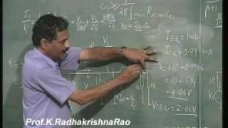
Lecture Series on Analog ICs by Prof. K. Radhakrishna Rao, Department of Electrical Engineering, IIT Madras. For more details on NPTEL visit http://nptel.iitm.ac.in
Lecture Series on Analog ICs by Prof. K. Radhakrishna Rao, Department of Electrical Engineering, IIT Madras. For more details on NPTEL visit http://nptel.iitm.ac.in

Lecture Series on Analog ICs by Prof. K. Radhakrishna Rao, Department of Electrical Engineering, IIT Madras. For more details on NPTEL visit http://nptel.iitm.ac.in

Lecture Series on Analog ICs by Prof. K. Radhakrishna Rao, Department of Electrical Engineering, IIT Madras. For more details on NPTEL visit http://nptel.iitm.ac.in

Lecture Series on Analog ICs by Prof. K. Radhakrishna Rao, Department of Electrical Engineering, IIT Madras. For more details on NPTEL visit http://nptel.iitm.ac.in

Lecture Series on Analog ICs by Prof. K. Radhakrishna Rao, Department of Electrical Engineering, IIT Madras. For more details on NPTEL visit http://nptel.iitm.ac.in
Lecture Series on Analog ICs by Prof. K.Radhakrishna Rao , Department of Electrical Engineering,I.I.T.Madras. For more details on NPTEL visit http://nptel.iitm.ac.in

Lecture Series on Analog ICs by Prof. K.Radhakrishna Rao , Department of Electrical Engineering,I.I.T.Madras. For more details on NPTEL visit http://nptel.iitm.ac.in
Lecture Series on Analog ICs by Prof. K.Radhakrishna Rao , Department of Electrical Engineering,I.I.T.Madras. For more details on NPTEL visit http://nptel.iitm.ac.in
Lecture Series on Analog ICs by Prof. K.Radhakrishna Rao , Department of Electrical Engineering,I.I.T.Madras. For more details on NPTEL visit http://nptel.iitm.ac.in

Lecture Series on Analog ICs by Prof. K.Radhakrishna Rao , Department of Electrical Engineering,I.I.T.Madras. For more details on NPTEL visit http://nptel.iitm.ac.in
Lecture Series on Analog ICs by Prof. K.Radhakrishna Rao , Department of Electrical Engineering,I.I.T.Madras. For more details on NPTEL visit http://nptel.iitm.ac.in
Lecture Series on Analog ICs by Prof. K.Radhakrishna Rao , Department of Electrical Engineering,I.I.T.Madras. For more details on NPTEL visit http://nptel.iitm.ac.in

Lecture Series on Analog ICs by Prof. K.Radhakrishna Rao , Department of Electrical Engineering,I.I.T.Madras. For more details on NPTEL visit http://nptel.iitm.ac.in
Lecture Series on Analog ICs by Prof. K.Radhakrishna Rao , Department of Electrical Engineering,I.I.T.Madras. For more details on NPTEL visit http://nptel.iitm.ac.in

Lecture Series on Analog ICs by Prof. K.Radhakrishna Rao , Department of Electrical Engineering,I.I.T.Madras. For more details on NPTEL visit http://nptel.iitm.ac.in

Lecture Series on Analog ICs by Prof. K.Radhakrishna Rao , Department of Electrical Engineering,I.I.T.Madras. For more details on NPTEL visit http://nptel.iitm.ac.in
Lecture Series on Analog ICs by Prof. K.Radhakrishna Rao , Department of Electrical Engineering,I.I.T.Madras. For more details on NPTEL visit http://nptel.iitm.ac.in

Lecture Series on Analog ICs by Prof. K.Radhakrishna Rao , Department of Electrical Engineering,I.I.T.Madras. For more details on NPTEL visit http://nptel.iitm.ac.in

Lecture Series on Analog ICs by Prof. K.Radhakrishna Rao , Department of Electrical Engineering,I.I.T.Madras. For more details on NPTEL visit http://nptel.iitm.ac.in

Lecture Series on Analog ICs by Prof. K.Radhakrishna Rao , Department of Electrical Engineering,I.I.T.Madras. For more details on NPTEL visit http://nptel.iitm.ac.in
Lecture Series on Analog ICs by Prof. K.Radhakrishna Rao , Department of Electrical Engineering,I.I.T.Madras. For more details on NPTEL visit http://nptel.iitm.ac.in
Lecture Series on Analog ICs by Prof. K.Radhakrishna Rao , Department of Electrical Engineering,I.I.T.Madras. For more details on NPTEL visit http://nptel.iitm.ac.in

Lecture Series on Analog ICs by Prof. K.Radhakrishna Rao , Department of Electrical Engineering,I.I.T.Madras. For more details on NPTEL visit http://nptel.iitm.ac.in
Lecture Series on Analog ICs by Prof. K.Radhakrishna Rao , Department of Electrical Engineering,I.I.T.Madras. For more details on NPTEL visit http://nptel.iitm.ac.in

Lecture Series on Analog ICs by Prof. K.Radhakrishna Rao , Department of Electrical Engineering,I.I.T.Madras. For more details on NPTEL visit http://nptel.iitm.ac.in
Lecture Series on Analog ICs by Prof. K.Radhakrishna Rao , Department of Electrical Engineering,I.I.T.Madras. For more details on NPTEL visit http://nptel.iitm.ac.in

Lecture Series on Analog ICs by Prof. K.Radhakrishna Rao , Department of Electrical Engineering,I.I.T.Madras. For more details on NPTEL visit http://nptel.iitm.ac.in

Lecture Series on Digital Integrated Circuits by Dr. Amitava Dasgupta, Department of Electrical Engineering,IIT Madras. For more details on NPTEL visit http://nptel.iitm.ac.in

Lecture Series on Digital Integrated Circuits by Dr. Amitava Dasgupta, Department of Electrical Engineering,IIT Madras. For more details on NPTEL visit http://nptel.iitm.ac.in
Lecture Series on Digital Integrated Circuits by Dr. Amitava Dasgupta, Department of Electrical Engineering,IIT Madras. For more details on NPTEL visit http://nptel.iitm.ac.in

Lecture Series on Digital Integrated Circuits by Dr. Amitava Dasgupta, Department of Electrical Engineering,IIT Madras. For more details on NPTEL visit http://nptel.iitm.ac.in.GaAs MESFET Characteristics and Equivalent Circuit

Lecture Series on Digital Integrated Circuits by Dr. Amitava Dasgupta, Department of Electrical Engineering,IIT Madras. For more details on NPTEL visit http://nptel.iitm.ac.in

Lecture Series on Digital Integrated Circuits by Dr. Amitava Dasgupta, Department of Electrical Engineering,IIT Madras. For more details on NPTEL visit http://nptel.iitm.ac.in
Lecture Series on Digital Integrated Circuits by Dr. Amitava Dasgupta, Department of Electrical Engineering,IIT Madras. For more details on NPTEL visit http://nptel.iitm.ac.in

Lecture Series on Digital Integrated Circuits by Dr. Amitava Dasgupta, Department of Electrical Engineering,IIT Madras. For more details on NPTEL visit http://nptel.iitm.ac.in
Lecture Series on Digital Integrated Circuits by Dr. Amitava Dasgupta, Department of Electrical Engineering,IIT Madras. For more details on NPTEL visit http://nptel.iitm.ac.in

Lecture Series on Digital Integrated Circuits by Dr. Amitava Dasgupta, Department of Electrical Engineering,IIT Madras. For more details on NPTEL visit http://nptel.iitm.ac.in

Lecture Series on Digital Integrated Circuits by Dr. Amitava Dasgupta, Department of Electrical Engineering,IIT Madras. For more details on NPTEL visit http://nptel.iitm.ac.in

Lecture Series on Digital Integrated Circuits by Dr. Amitava Dasgupta, Department of Electrical Engineering,IIT Madras. For more details on NPTEL visit http://nptel.iitm.ac.in

Lecture Series on Digital Integrated Circuits by Dr. Amitava Dasgupta, Department of Electrical Engineering,IIT Madras. For more details on NPTEL visit http://nptel.iitm.ac.in.Dynamic CMOS ;Transmission Gates;Realization Of MUX,Decoder,D-F/F

Lecture Series on Digital Integrated Circuits by Dr. Amitava Dasgupta, Department of Electrical Engineering,IIT Madras. For more details on NPTEL visit http://nptel.iitm.ac.in

Lecture Series on Digital Integrated Circuits by Dr. Amitava Dasgupta, Department of Electrical Engineering,IIT Madras. For more details on NPTEL visit http://nptel.iitm.ac.in

Lecture Series on Digital Integrated Circuits by Dr. Amitava Dasgupta, Department of Electrical Engineering,IIT Madras. For more details on NPTEL visit http://nptel.iitm.ac.in

Lecture Series on Digital Integrated Circuits by Dr. Amitava Dasgupta, Department of Electrical Engineering,IIT Madras. For more details on NPTEL visit http://nptel.iitm.ac.in
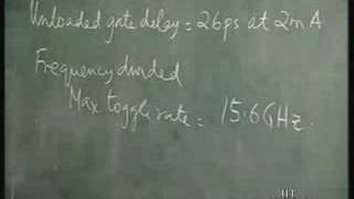
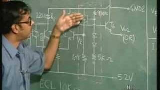
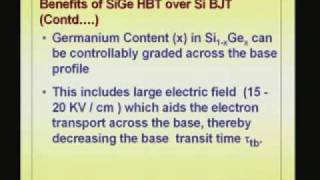
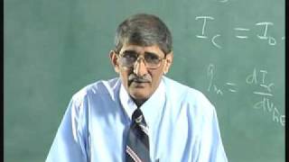
Lecture Series on Digital Integrated Circuits by Dr. Amitava Dasgupta, Department of Electrical Engineering,IIT Madras. For more details on NPTEL visit http://nptel.iitm.ac.in.Heterojunction Bipolar Transistor Based ECL; ECL Gate Array
Lecture Series on Digital Integrated Circuits by Dr. Amitava Dasgupta, Department of Electrical Engineering,IIT Madras. For more details on NPTEL visit http://nptel.iitm.ac.in.Polyemitter Bipolar Transistor In ECL; Propagation Delay
Lecture Series on Digital Integrated Circuits by Dr. Amitava Dasgupta, Department of Electrical Engineering,IIT Madras. For more details on NPTEL visit http://nptel.iitm.ac.in.Emitter Function Logic;Low Power ECL;Current Mirror Control Logic.

Lecture Series on Digital Integrated Circuits by Dr. Amitava Dasgupta , Department of Electrical Engineering, IIT Madras. For more details on NPTEL visit http://nptel.iitm.ac.in
Lecture Series on Digital Integrated Circuits by Dr. Amitava Dasgupta , Department of Electrical Engineering, IIT Madras. For more details on NPTEL visit http://nptel.iitm.ac.in
Lecture Series on Digital Integrated Circuits by Dr. Amitava Dasgupta , Department of Electrical Engineering, IIT Madras. For more details on NPTEL visit http://nptel.iitm.ac.in

Lecture Series on Digital Integrated Circuits by Dr. Amitava Dasgupta , Department of Electrical Engineering, IIT Madras. For more details on NPTEL visit http://nptel.iitm.ac.in. Lecture Title: Stacked I-square L ; I- square L - TTL Interfacing

Lecture Series on Digital Integrated Circuits by Dr. Amitava Dasgupta , Department of Electrical Engineering, IIT Madras. For more details on NPTEL visit http://nptel.iitm.ac.in. Lecture Title: Schottky Transistor Logic; Heterojunction I-square L.
Lecture Series on Digital Integrated Circuits by Dr. Amitava Dasgupta , Department of Electrical Engineering, IIT Madras. For more details on NPTEL visit http://nptel.iitm.ac.in

Lecture Series on Digital Integrated Circuits by Dr. Amitava Dasgupta , Department of Electrical Engineering, IIT Madras. For more details on NPTEL visit http://nptel.iitm.ac.in. I-square L - Condition for Proper Operation; Noise margin

Lecture Series on Digital Integrated Circuits by Dr. Amitava Dasgupta , Department of Electrical Engineering, IIT Madras. For more details on NPTEL visit http://nptel.iitm.ac.in. Lecture Title: Edge triggered D-F/F and Decoder realization Using I-square L

Lecture Series on Digital Integrated Circuits by Dr. Amitava Dasgupta , Department of Electrical Engineering, IIT Madras. For more details on NPTEL visit http://nptel.iitm.ac.in
Lecture Series on Digital Integrated Circuits by Dr. Amitava Dasgupta , Department of Electrical Engineering, IIT Madras. For more details on NPTEL visit http://nptel.iitm.ac.in

Lecture Series on Digital Integrated Circuits by Dr . Amitava Dasgupta, Department of Electrical Engineering,IIT Madras. For more details on NPTEL visit http://nptel.iitm.ac.in

Lecture Series on Digital Integrated Circuits by Dr . Amitava Dasgupta, Department of Electrical Engineering,IIT Madras. For more details on NPTEL visit http://nptel.iitm.ac.in

Lecture Series on Digital Integrated Circuits by Dr . Amitava Dasgupta, Department of Electrical Engineering,IIT Madras. For more details on NPTEL visit http://nptel.iitm.ac.in
Lecture Series on Digital Integrated Circuits by Dr . Amitava Dasgupta, Department of Electrical Engineering,IIT Madras. For more details on NPTEL visit http://nptel.iitm.ac.in

Lecture Series on Digital Integrated Circuits by Dr . Amitava Dasgupta, Department of Electrical Engineering,IIT Madras. For more details on NPTEL visit http://nptel.iitm.ac.in. Lecture Title:Schottky Transistor Introduction to Bipolar Logic Circuits
Lecture Series on Digital Integrated Circuits by Dr . Amitava Dasgupta, Department of Electrical Engineering,IIT Madras. For more details on NPTEL visit http://nptel.iitm.ac.in
Lecture Series on Digital Integrated Circuits by Dr . Amitava Dasgupta, Department of Electrical Engineering,IIT Madras. For more details on NPTEL visit http://nptel.iitm.ac.in

Lecture Series on Digital Integrated Circuits by Dr . Amitava Dasgupta, Department of Electrical Engineering,IIT Madras. For more details on NPTEL visit http://nptel.iitm.ac.in

Lecture Series on Digital Integrated Circuits by Dr . Amitava Dasgupta, Department of Electrical Engineering,IIT Madras. For more details on NPTEL visit http://nptel.iitm.ac.in

Lecture Series on Digital Integrated Circuits by Dr . Amitava Dasgupta, Department of Electrical Engineering,IIT Madras. For more details on NPTEL visit http://nptel.iitm.ac.in

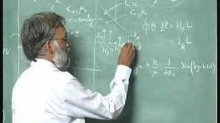
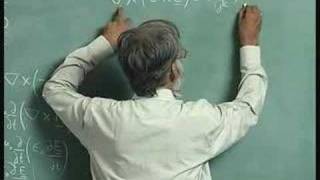
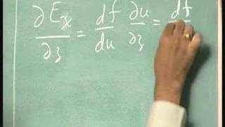
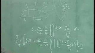
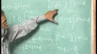
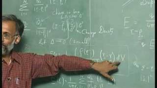
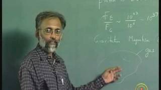
Electro Magnetic Field

Electro Magnetic Field
Electro Magnetic Field
Electro Magnetic Field
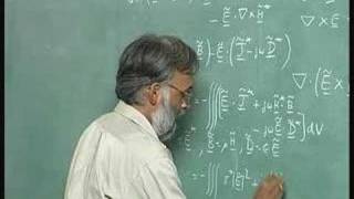
Electro Magnetic Field

Electro Magnetic Field

Lecture series on Electro Magnetic Field, by Prof. Harishankar Ramachandran, Dept of Electrical Engineering, IIT Madras
Electro Magnetic Field

Electro Magnetic Field
Electro Magnetic Field
Electro Magnetic Field

Electro Magnetic Field

Electro Magnetic Field
Electro Magnetic Field
Electro Magnetic Field

Electro Magnetic Field

Electro Magnetic Field
Electro Magnetic Field

Electro Magnetic Field
Electro Magnetic Field

Electro Magnetic Field

Electro Magnetic Field

Electro Magnetic Field

Electro Magnetic Field

Electro Magnetic Field

Electro Magnetic Field
Electro Magnetic Field

Electro Magnetic Field

Electro Magnetic Field
Electro Magnetic Field

Lecture series on Electro Magnetic Field, by Prof. Harishankar Ramachandran, Dept of Electrical Engineering, IIT Madras

Electro Magnetic Field
Electro Magnetic Field
Electro Magnetic Field

Electro Magnetic Field

Electro Magnetic Field

Electro Magnetic Field

Electro Magnetic Field
Electro Magnetic Field
Electro Magnetic Field

Electro Magnetic Field

Electro Magnetic Field
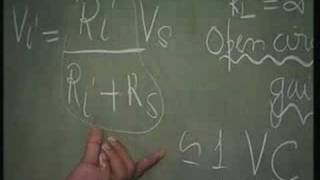
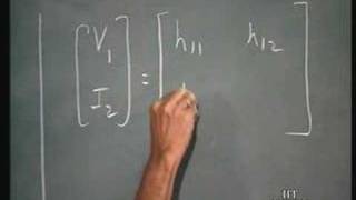
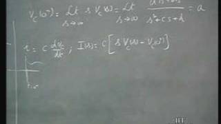
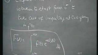
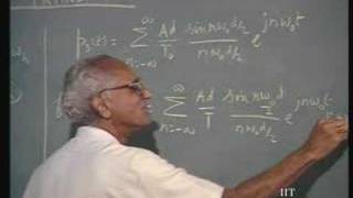
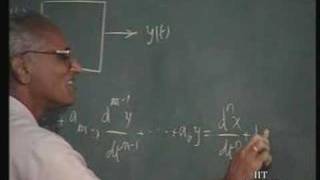
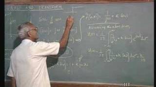
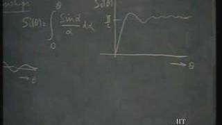
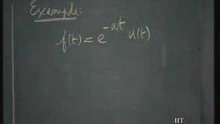
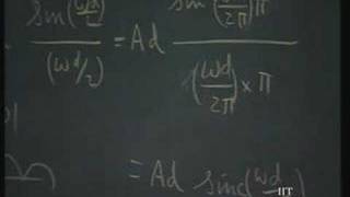
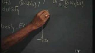
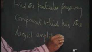
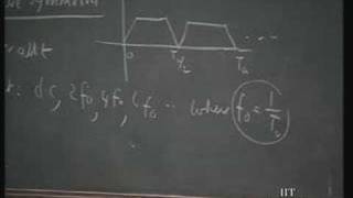
Lecture Series on Networks and Systems by Prof.V.G.K.Murti, Department of Electrical Engineering, IIT Madras. For More details on NPTEL visit http://nptel.iitm.ac.in
Lecture Series on Networks and Systems by Prof. V.G.K.Murti, Department of Electrical Engineering,IIT Madras. For more details on NPTEL visit http://nptel.iitm.ac.in
Lecture Series on Networks and Systems by Prof.V.G.K.Murti, Department of Electrical Engineering, IIT Madras. For More details on NPTEL visit http://nptel.iitm.ac.in

Lecture Series on Networks and Systems by Prof.V.G.K.Murti, Department of Electrical Engineering, IIT Madras. For More details on NPTEL visit http://nptel.iitm.ac.in
Lecture Series on Networks and Systems by Prof.V.G.K.Murti, Department of Electrical Engineering, IIT Madras. For More details on NPTEL visit http://nptel.iitm.ac.in

Lecture Series on Networks and Systems by Prof.V.G.K.Murti, Department of Electrical Engineering, IIT Madras. For More details on NPTEL visit http://nptel.iitm.ac.in
Lecture Series on Networks and Systems by Prof.V.G.K.Murti, Department of Electrical Engineering, IIT Madras. For More details on NPTEL visit http://nptel.iitm.ac.in

Lecture Series on Networks and Systems by Prof. V.G.K.Murti, Department of Electrical Engineering,IIT Madras. For more details on NPTEL visit http://nptel.iitm.ac.in
Lecture Series on Networks and Systems by Prof. V.G.K.Murti, Department of Electrical Engineering,IIT Madras. For more details on NPTEL visit http://nptel.iitm.ac.in

Lecture Series on Networks and Systems by Prof. V.G.K.Murti, Department of Electrical Engineering,IIT Madras. For more details on NPTEL visit http://nptel.iitm.ac.in

Lecture Series on Networks and Systems by Prof. V.G.K.Murti, Department of Electrical Engineering,IIT Madras. For more details on NPTEL visit http://nptel.iitm.ac.in

Lecture Series on Networks and Systems by Prof. V.G.K.Murti, Department of Electrical Engineering,IIT Madras. For more details on NPTEL visit http://nptel.iitm.ac.in

Lecture Series on Networks and Systems by Prof. V.G.K.Murti, Department of Electrical Engineering,IIT Madras. For more details on NPTEL visit http://nptel.iitm.ac.in

Lecture Series on Networks and Systems by Prof. V.G.K.Murti, Department of Electrical Engineering,IIT Madras. For more details on NPTEL visit http://nptel.iitm.ac.in

Lecture Series on Networks and Systems by Prof. V.G.K.Murti, Department of Electrical Engineering,IIT Madras. For more details on NPTEL visit http://nptel.iitm.ac.in

Lecture Series on Networks and Systems by Prof. V.G.K.Murti, Department of Electrical Engineering,IIT Madras. For more details on NPTEL visit http://nptel.iitm.ac.in

Lecture Series on Networks and Systems by Prof. V.G.K.Murti, Department of Electrical Engineering,IIT Madras. For more details on NPTEL visit http://nptel.iitm.ac.in

Lecture Series on Networks and Systems by Prof. V.G.K.Murti, Department of Electrical Engineering,IIT Madras. For more details on NPTEL visit http://nptel.iitm.ac.in

Lecture Series on Networks and Systems by Prof.V.G.K.Murti, Department of Electrical Engineering, IIT Madras. For More details on NPTEL visit http://nptel.iitm.ac.in
Lecture Series on Networks and Systems by Prof.V.G.K.Murti, Department of Electrical Engineering, IIT Madras. For More details on NPTEL visit http://nptel.iitm.ac.in

Lecture Series on Networks and Systems by Prof. V.G.K.Murti, Department of Electrical Engineering,IIT Madras. For more details on NPTEL visit http://nptel.iitm.ac.in

Lecture Series on Networks and Systems by Prof. V.G.K.Murti, Department of Electrical Engineering,IIT Madras. For more details on NPTEL visit http://nptel.iitm.ac.in

Lecture Series on Networks and Systems by Prof.V.G.K.Murti, Department of Electrical Engineering, IIT Madras. For More details on NPTEL visit http://nptel.iitm.ac.in
Lecture Series on Networks and Systems by Prof.V.G.K.Murti, Department of Electrical Engineering, IIT Madras. For More details on NPTEL visit http://nptel.iitm.ac.in

Lecture Series on Networks and Systems by Prof.V.G.K.Murti, Department of Electrical Engineering, IIT Madras. For More details on NPTEL visit http://nptel.iitm.ac.in

Lecture Series on Networks and Systems by Prof.V.G.K.Murti, Department of Electrical Engineering, IIT Madras. For More details on NPTEL visit http://nptel.iitm.ac.in

Lecture Series on Networks and Systems by Prof.V.G.K.Murti, Department of Electrical Engineering, IIT Madras. For More details on NPTEL visit http://nptel.iitm.ac.in
Lecture Series on Networks and Systems by Prof.V.G.K.Murti, Department of Electrical Engineering, IIT Madras. For More details on NPTEL visit http://nptel.iitm.ac.in
Lecture Series on Networks and Systems by Prof.V.G.K.Murti, Department of Electrical Engineering, IIT Madras. For More details on NPTEL visit http://nptel.iitm.ac.in
Lecture Series on Networks and Systems by Prof.V.G.K.Murti, Department of Electrical Engineering, IIT Madras. For More details on NPTEL visit http://nptel.iitm.ac.in
Lecture Series on Networks and Systems by Prof.V.G.K.Murti, Department of Electrical Engineering, IIT Madras. For More details on NPTEL visit http://nptel.iitm.ac.in
Lecture Series on Networks and Systems by Prof.V.G.K.Murti, Department of Electrical Engineering, IIT Madras. For More details on NPTEL visit http://nptel.iitm.ac.in
Lecture Series on Networks and Systems by Prof.V.G.K.Murti, Department of Electrical Engineering, IIT Madras. For More details on NPTEL visit http://nptel.iitm.ac.in
Lecture Series on Networks and Systems by Prof. V.G.K.Murti, Department of Electrical Engineering,IIT Madras. For more details on NPTEL visit http://nptel.iitm.ac.in
Lecture Series on Networks and Systems by Prof. V.G.K.Murti, Department of Electrical Engineering,IIT Madras. For more details on NPTEL visit http://nptel.iitm.ac.in
Lecture Series on Networks and Systems by Prof. V.G.K.Murti, Department of Electrical Engineering,IIT Madras. For more details on NPTEL visit http://nptel.iitm.ac.in

Lecture Series on Networks and Systems by Prof. V.G.K.Murti, Department of Electrical Engineering,IIT Madras. For more details on NPTEL visit http://nptel.iitm.ac.in

Lecture Series on Networks and Systems by Prof. V.G.K.Murti, Department of Electrical Engineering,IIT Madras. For more details on NPTEL visit http://nptel.iitm.ac.in

Lecture Series on Networks and Systems by Prof. V.G.K.Murti, Department of Electrical Engineering,IIT Madras. For more details on NPTEL visit http://nptel.iitm.ac.in
Lecture Series on Networks and Systems by Prof. V.G.K.Murti, Department of Electrical Engineering,IIT Madras. For more details on NPTEL visit http://nptel.iitm.ac.in

Lecture Series on Networks and Systems by Prof. V.G.K.Murti, Department of Electrical Engineering,IIT Madras. For more details on NPTEL visit http://nptel.iitm.ac.in

Lecture Series on Networks and Systems by Prof. V.G.K.Murti, Department of Electrical Engineering,IIT Madras. For more details on NPTEL visit http://nptel.iitm.ac.in
Lecture Series on Networks and Systems by Prof. V.G.K.Murti, Department of Electrical Engineering,IIT Madras. For more details on NPTEL visit http://nptel.iitm.ac.in

Lecture Series on Networks and Systems by Prof. V.G.K.Murti, Department of Electrical Engineering,IIT Madras. For more details on NPTEL visit http://nptel.iitm.ac.in
Lecture Series on Networks and Systems by Prof. V.G.K.Murti, Department of Electrical Engineering,IIT Madras. For more details on NPTEL visit http://nptel.iitm.ac.in

Lecture Series on Networks and Systems by Prof. V.G.K.Murti, Department of Electrical Engineering,IIT Madras. For more details on NPTEL visit http://nptel.iitm.ac.in
High Speed Devices&Circuits

High Speed Devices&Circuits

High Speed Devices&Circuits
High Speed Devices&Circuits
High Speed Devices&Circuits
High Speed Devices&Circuits

High Speed Devices&Circuits

High Speed Devices&Circuits
High Speed Devices&Circuits

High Speed Devices& Circuits
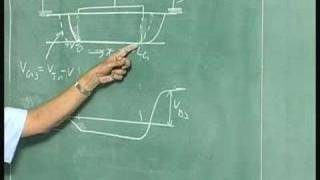
High Speed Devices&Circuits
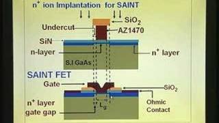
High Speed Devices&Circuits

High Speed Devices and Circuits
High Speed Devices and Circuits

High SPeed Devices and Circuits

High SPeed DEvices and Circuits
High Speed Devices and Circuits

High Speed Devices and Circuits
High Speed Devices and Circuits

High Speed devices and Circuits

High Speed Devices and Circuits
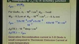
High Speed Devices and Circuits

High Speed Devices and Circuits
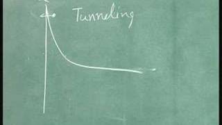
High Speed Devices and Circuits

High Speed Devices and circuits Lecture 15 - Ohmic Contacts on Semiconductors

High Speed Devices and Circuits Lecture14- Metal Semiconductor contacts for MESFET (Contd.)
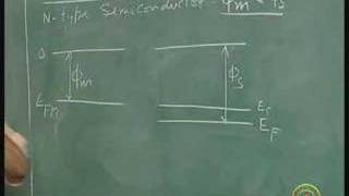
High Speed devices and Circuits - Lecture13- Metal Semiconductor contacts for MESFET (Contd.)
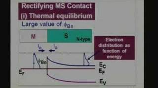
High Speed Devices and Circuits - Metal Semiconductor contacts for MESFET
High Speed Devices and Circuits

High Speed Devices and Circuits - MBE and LPE for GaAs Epitaxy

High Speed Devices and Circuits - Epitaxial Tech. for GaAs High Speed Devices

Brief Overview of GaAs Technology for High Speed Devices
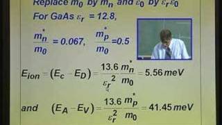
High Speed Devices and Circuits - Crystal Structures in GaAs
High Speed Devices and Circuits - Crystal Structures in GaAs
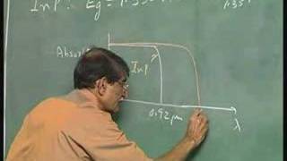
High Speed Devices and Circuits - Temary Compound Semiconductor and their Application

High Speed Devices and Circuits - Temary Compound Semiconductor and their Application

High Speed devices and Circuits Classifications & Properties of Compound Semiconductors
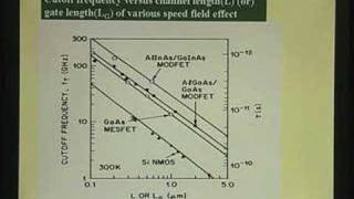
Requirements of High Speed Devices, Circuits & Materials

High Speed Devices and Circuits Introduction to Basic Concepts

VLSI Data Conversion Circuits by Dr. Shanthi Pavan, Department of Electrical Engineering, IIT Madras. For more details on NPTEL visit http://nptel.iitm.ac.in

VLSI Data Conversion Circuits by Dr. Shanthi Pavan, Department of Electrical Engineering, IIT Madras. For more details on NPTEL visit http://nptel.iitm.ac.in

VLSI Data Conversion Circuits by Dr. Shanthi Pavan, Department of Electrical Engineering, IIT Madras. For more details on NPTEL visit http://nptel.iitm.ac.in

VLSI Data Conversion Circuits by Dr. Shanthi Pavan, Department of Electrical Engineering, IIT Madras. For more details on NPTEL visit http://nptel.iitm.ac.in

VLSI Data Conversion Circuits by Dr. Shanthi Pavan, Department of Electrical Engineering, IIT Madras. For more details on NPTEL visit http://nptel.iitm.ac.in

VLSI Data Conversion Circuits by Dr. Shanthi Pavan, Department of Electrical Engineering, IIT Madras. For more details on NPTEL visit http://nptel.iitm.ac.in
VLSI Data Conversion Circuits by Dr. Shanthi Pavan, Department of Electrical Engineering, IIT Madras. For more details on NPTEL visit http://nptel.iitm.ac.in

VLSI Data Conversion Circuits by Dr. Shanthi Pavan, Department of Electrical Engineering, IIT Madras. For more details on NPTEL visit http://nptel.iitm.ac.in

VLSI Data Conversion Circuits by Dr. Shanthi Pavan, Department of Electrical Engineering, IIT Madras. For more details on NPTEL visit http://nptel.iitm.ac.in

VLSI Data Conversion Circuits by Dr. Shanthi Pavan, Department of Electrical Engineering, IIT Madras. For more details on NPTEL visit http://nptel.iitm.ac.in
VLSI Data Conversion Circuits by Dr. Shanthi Pavan, Department of Electrical Engineering, IIT Madras. For more details on NPTEL visit http://nptel.iitm.ac.in
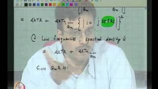
VLSI Data Conversion Circuits by Dr. Shanthi Pavan, Department of Electrical Engineering, IIT Madras. For more details on NPTEL visit http://nptel.iitm.ac.in
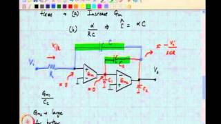
VLSI Data Conversion Circuits by Dr. Shanthi Pavan, Department of Electrical Engineering, IIT Madras. For more details on NPTEL visit http://nptel.iitm.ac.in
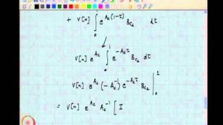
VLSI Data Conversion Circuits by Dr. Shanthi Pavan, Department of Electrical Engineering, IIT Madras. For more details on NPTEL visit http://nptel.iitm.ac.in

VLSI Data Conversion Circuits by Dr. Shanthi Pavan, Department of Electrical Engineering, IIT Madras. For more details on NPTEL visit http://nptel.iitm.ac.in

VLSI Data Conversion Circuits by Dr. Shanthi Pavan, Department of Electrical Engineering, IIT Madras. For more details on NPTEL visit http://nptel.iitm.ac.in
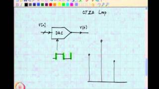
VLSI Data Conversion Circuits by Dr. Shanthi Pavan, Department of Electrical Engineering, IIT Madras. For more details on NPTEL visit http://nptel.iitm.ac.in
VLSI Data Conversion Circuits by Dr. Shanthi Pavan, Department of Electrical Engineering, IIT Madras. For more details on NPTEL visit http://nptel.iitm.ac.in
VLSI Data Conversion Circuits by Dr. Shanthi Pavan, Department of Electrical Engineering, IIT Madras. For more details on NPTEL visit http://nptel.iitm.ac.in

VLSI Data Conversion Circuits by Dr. Shanthi Pavan, Department of Electrical Engineering, IIT Madras. For more details on NPTEL visit http://nptel.iitm.ac.in
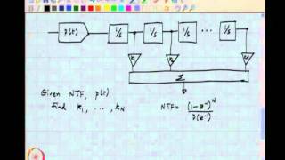
VLSI Data Conversion Circuits by Dr. Shanthi Pavan, Department of Electrical Engineering, IIT Madras. For more details on NPTEL visit http://nptel.iitm.ac.in

VLSI Data Conversion Circuits by Dr. Shanthi Pavan, Department of Electrical Engineering, IIT Madras. For more details on NPTEL visit http://nptel.iitm.ac.in

VLSI Data Conversion Circuits by Dr. Shanthi Pavan, Department of Electrical Engineering, IIT Madras. For more details on NPTEL visit http://nptel.iitm.ac.in

VLSI Data Conversion Circuits by Dr. Shanthi Pavan, Department of Electrical Engineering, IIT Madras. For more details on NPTEL visit http://nptel.iitm.ac.in
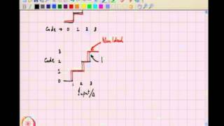
VLSI Data Conversion Circuits by Dr. Shanthi Pavan, Department of Electrical Engineering, IIT Madras. For more details on NPTEL visit http://nptel.iitm.ac.in

VLSI Data Conversion Circuits by Dr. Shanthi Pavan, Department of Electrical Engineering, IIT Madras. For more details on NPTEL visit http://nptel.iitm.ac.in
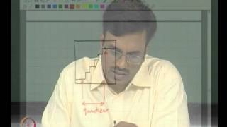
VLSI Data Conversion Circuits by Dr. Shanthi Pavan, Department of Electrical Engineering, IIT Madras. For more details on NPTEL visit http://nptel.iitm.ac.in
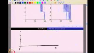
VLSI Data Conversion Circuits by Dr. Shanthi Pavan, Department of Electrical Engineering, IIT Madras. For more details on NPTEL visit http://nptel.iitm.ac.in

VLSI Data Conversion Circuits by Dr. Shanthi Pavan, Department of Electrical Engineering, IIT Madras. For more details on NPTEL visit http://nptel.iitm.ac.in

VLSI Data Conversion Circuits by Dr. Shanthi Pavan, Department of Electrical Engineering, IIT Madras. For more details on NPTEL visit http://nptel.iitm.ac.in

VLSI Data Conversion Circuits by Dr. Shanthi Pavan, Department of Electrical Engineering, IIT Madras. For more details on NPTEL visit http://nptel.iitm.ac.in

VLSI Data Conversion Circuits by Dr. Shanthi Pavan, Department of Electrical Engineering, IIT Madras. For more details on NPTEL visit http://nptel.iitm.ac.in

VLSI Data Conversion Circuits by Dr. Shanthi Pavan, Department of Electrical Engineering, IIT Madras. For more details on NPTEL visit http://nptel.iitm.ac.in
VLSI Data Conversion Circuits by Dr. Shanthi Pavan, Department of Electrical Engineering, IIT Madras. For more details on NPTEL visit http://nptel.iitm.ac.in
VLSI Data Conversion Circuits by Dr. Shanthi Pavan, Department of Electrical Engineering, IIT Madras. For more details on NPTEL visit http://nptel.iitm.ac.in
VLSI Data Conversion Circuits by Dr. Shanthi Pavan, Department of Electrical Engineering, IIT Madras. For more details on NPTEL visit http://nptel.iitm.ac.in

VLSI Data Conversion Circuits by Dr. Shanthi Pavan, Department of Electrical Engineering, IIT Madras. For more details on NPTEL visit http://nptel.iitm.ac.in

VLSI Data Conversion Circuits by Dr. Shanthi Pavan, Department of Electrical Engineering, IIT Madras. For more details on NPTEL visit http://nptel.iitm.ac.in

VLSI Data Conversion Circuits by Dr. Shanthi Pavan, Department of Electrical Engineering, IIT Madras. For more details on NPTEL visit http://nptel.iitm.ac.in
VLSI Data Conversion Circuits by Dr. Shanthi Pavan, Department of Electrical Engineering, IIT Madras. For more details on NPTEL visit http://nptel.iitm.ac.in

VLSI Data Conversion Circuits by Dr. Shanthi Pavan, Department of Electrical Engineering, IIT Madras. For more details on NPTEL visit http://nptel.iitm.ac.in
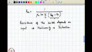
VLSI Data Conversion Circuits by Dr. Shanthi Pavan, Department of Electrical Engineering, IIT Madras. For more details on NPTEL visit http://nptel.iitm.ac.in

VLSI Data Conversion Circuits by Dr. Shanthi Pavan, Department of Electrical Engineering, IIT Madras. For more details on NPTEL visit http://nptel.iitm.ac.in
VLSI Data Conversion Circuits by Dr. Shanthi Pavan, Department of Electrical Engineering, IIT Madras. For more details on NPTEL visit http://nptel.iitm.ac.in
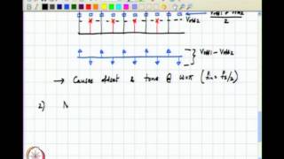
VLSI Data Conversion Circuits by Dr. Shanthi Pavan, Department of Electrical Engineering, IIT Madras. For more details on NPTEL visit http://nptel.iitm.ac.in

VLSI Data Conversion Circuits by Dr. Shanthi Pavan, Department of Electrical Engineering, IIT Madras. For more details on NPTEL visit http://nptel.iitm.ac.in

VLSI Data Conversion Circuits by Dr. Shanthi Pavan, Department of Electrical Engineering, IIT Madras. For more details on NPTEL visit http://nptel.iitm.ac.in

Video Lecture Series by IIT Professors ( Not Available in NPTEL)
VLSI Broadband Communication Circuits
By Prof. Nagendra Krishnapura
For more video Lectures .... www.satishkashyap.com
For free ebooks ...... www.ebook29.blogspot.com
1. Introduction to broadband digital communication
2. Introduction to broadband digital communication
3. Serializers and deserializers
4. Forgot to hit "record"!
5. CMOS logic, single ended data transmission, limitations
6. Current mode logic-basic circuit design
7. Current mode logic-MUX, XOR, latch
8. Current mode logic-latch design
9. Current mode logic-latch characteristics
10. Low pass transmission channel-Intersymbol interference, error rate
11. First order channel model, ISI
12. ISI, jitter, eye opening
13. Channel characteristics-Intersymbol interference, Crosstalk
14. Equalizer design
15. Equalizer design-minimizing the residual error
16. Equalization-Effect on noise and crosstalk
17. Tradeoffs between equalization at Tx and Rx; Design of Tx equalizers
18. Design of Transmit equalizers using flip-flops and transconductors
19. Tx equalizer-design considerations
20. Tx equalizer-design considerations; realizing variable coefficients
21. Differential pair-effect of tail node capacitance; Continuous time equalization
22. Continuous-time equalizer realization; replica biasing for the tail current source
23. Assignment 2 discussion
24. Replica biasing, optimizing transmitter swing
25. Replica biasing, optimizing transmitter swing
26. Analog layout optimization; Equalization at the receiver
27. Equalization at the receiver; Basics of adaptation
28. LMS adaptation
29. Sign-sign LMS adaptation
30. LMS implementation details
31. Adaptive equalizer implementation, S/H based equalizer, obtaining the gradients
32. Mid term discussion; Multiplexed and demultiplexed PRBS sequences; Latch vs. amplifier; Zeros for pre- and post- cursor equalization; Echo cancellation
33. Decision feedback equalizers-elimination of noise enhancement; Error propagation
34. Decision feedback equalizers-bit error rate
35. Decision feedback equalizers-implementation issues
36. Assignment 3 discussion
37. Decision feedback equalizers-implementation issues
38. Introduction to clock and data recovery-Frequency multiplication using a phase locked loop
39. Type I PLL; derivation of the phase model of the PLL; Tri state phase detector
40. (continued) Type I PLL; derivation of the phase model of the PLL; Tri state phase detector
41. Type I PLL; Reference feedthrough; Tradeoff between reference feedthrough and lock range
42. Stability of feedback loops; Derivation of the type II PLL
43. Realization of type II PLLs-charge pump, loop filter
44. Reference feedthrough in a type II PLL; Phase detector for random data
45. Linear phase detector for random data
46. Linear phase detector; Transfer functions in a PLL
47. PLL review
48. Binary phase detectors; bang bang jitter
49. Miscellaneous topics-Optimal equalizers; Linearity assumption of PLL model; PLL capture phenomenon; Hogge phase detector offset correction
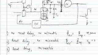
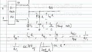
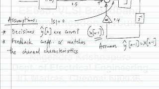
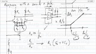
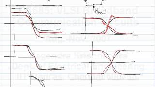
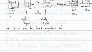
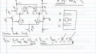
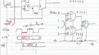
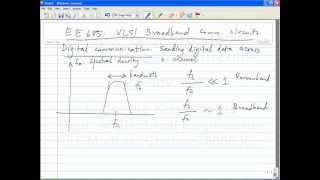
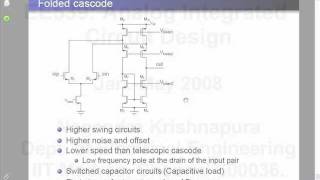
Analog Integrated Circuit Design by Prof.Nagendra Krishnapura sir

Analog Integrated Circuit Design by Prof.Nagendra Krishnapura sir

Analog Integrated Circuit Design by Prof.Nagendra Krishnapura sir

Analog Integrated Circuit Design by Prof.Nagendra Krishnapura sir
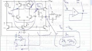
Analog Integrated Circuit Design by Prof.Nagendra Krishnapura sir

Analog Integrated Circuit Design by Prof.Nagendra Krishnapura sir

Analog Integrated Circuit Design by Prof.Nagendra Krishnapura sir

Analog Integrated Circuit Design by Prof.Nagendra Krishnapura sir

Analog Integrated Circuit Design by Prof.Nagendra Krishnapura sir

Analog Integrated Circuit Design by Prof.Nagendra Krishnapura sir

Analog Integrated Circuit Design by Prof.Nagendra Krishnapura sir
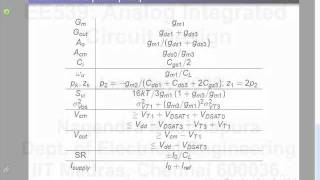
Analog Integrated Circuit Design by Prof.Nagendra Krishnapura sir

Analog Integrated Circuit Design by Prof.Nagendra Krishnapura sir

Analog Integrated Circuit Design by Prof.Nagendra Krishnapura sir

Analog Integrated Circuit Design by Prof.Nagendra Krishnapura sir

Analog Integrated Circuit Design by Prof.Nagendra Krishnapura sir

Analog Integrated Circuit Design by Prof.Nagendra Krishnapura sir

Analog Integrated Circuit Design by Prof.Nagendra Krishnapura sir
Analog Integrated Circuit Design by Prof.Nagendra Krishnapura sir

Analog Integrated Circuit Design by Prof.Nagendra Krishnapura sir
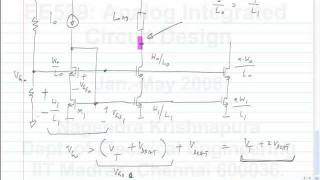
Analog Integrated Circuit Design by Prof.Nagendra Krishnapura sir
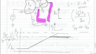
Analog Integrated Circuit Design by Prof.Nagendra Krishnapura sir

Analog Integrated Circuit Design by Prof.Nagendra Krishnapura sir

Analog Integrated Circuit Design by Prof.Nagendra Krishnapura sir

Analog Integrated Circuit Design by Prof.Nagendra Krishnapura sir

Analog Integrated Circuit Design by Prof.Nagendra Krishnapura sir

Analog Integrated Circuit Design by Prof.Nagendra Krishnapura sir
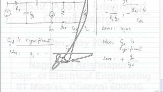
Analog Integrated Circuit Design by Prof.Nagendra Krishnapura sir

Analog Integrated Circuit Design by Prof.Nagendra Krishnapura sir

Analog Integrated Circuit Design by Prof.Nagendra Krishnapura sir
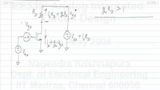
Analog Integrated Circuit Design by Prof.Nagendra Krishnapura sir

Analog Integrated Circuit Design by Prof.Nagendra Krishnapura sir

Analog Integrated Circuit Design by Prof.Nagendra Krishnapura sir
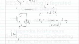
Analog Integrated Circuit Design by Prof.Nagendra Krishnapura sir

Analog Integrated Circuit Design by Prof.Nagendra Krishnapura sir
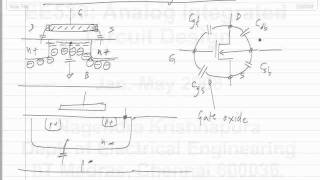
Analog Integrated Circuit Design by Prof.Nagendra Krishnapura sir

Analog Integrated Circuit Design by Prof.Nagendra Krishnapura sir
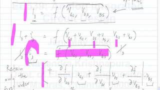
Analog Integrated Circuit Design by Prof.Nagendra Krishnapura sir

Analog Integrated Circuit Design by Prof.Nagendra Krishnapura sir
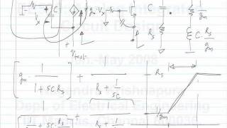
Analog Integrated Circuit Design by Prof.Nagendra Krishnapura sir
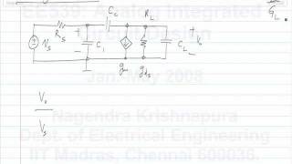
Analog Integrated Circuit Design by Prof.Nagendra Krishnapura sir

Analog Integrated Circuit Design by Prof.Nagendra Krishnapura sir

Analog Integrated Circuit Design by Prof.Nagendra Krishnapura sir
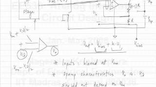
Analog Integrated Circuit Design by Prof.Nagendra Krishnapura sir

Analog Integrated Circuit Design by Prof.Nagendra Krishnapura sir

Analog Integrated Circuit Design by Prof.Nagendra Krishnapura sir
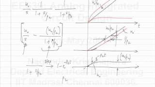
Analog Integrated Circuit Design by Prof.Nagendra Krishnapura sir

Analog Integrated Circuit Design by Prof.Nagendra Krishnapura sir
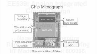
Analog Integrated Circuit Design by Prof.Nagendra Krishnapura sir
Analog IC Design by Dr. Nagendra Krishnapura, Department of Electronics & Communication Engineering, IIT Madras. For more details on NPTEL visit http://nptel.iitm.ac.in

Analog IC Design by Dr. Nagendra Krishnapura, Department of Electronics & Communication Engineering, IIT Madras. For more details on NPTEL visit http://nptel.iitm.ac.in

Analog IC Design by Dr. Nagendra Krishnapura, Department of Electronics & Communication Engineering, IIT Madras. For more details on NPTEL visit http://nptel.iitm.ac.in
Analog IC Design by Dr. Nagendra Krishnapura, Department of Electronics & Communication Engineering, IIT Madras. For more details on NPTEL visit http://nptel.iitm.ac.in
Analog IC Design by Dr. Nagendra Krishnapura, Department of Electronics & Communication Engineering, IIT Madras. For more details on NPTEL visit http://nptel.iitm.ac.in
Analog IC Design by Dr. Nagendra Krishnapura, Department of Electronics & Communication Engineering, IIT Madras. For more details on NPTEL visit http://nptel.iitm.ac.in

Analog IC Design by Dr. Nagendra Krishnapura, Department of Electronics & Communication Engineering, IIT Madras. For more details on NPTEL visit http://nptel.iitm.ac.in
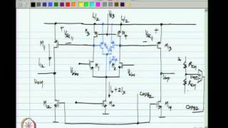
Analog IC Design by Dr. Nagendra Krishnapura, Department of Electronics & Communication Engineering, IIT Madras. For more details on NPTEL visit http://nptel.iitm.ac.in

Analog IC Design by Dr. Nagendra Krishnapura, Department of Electronics & Communication Engineering, IIT Madras. For more details on NPTEL visit http://nptel.iitm.ac.in

Analog IC Design by Dr. Nagendra Krishnapura, Department of Electronics & Communication Engineering, IIT Madras. For more details on NPTEL visit http://nptel.iitm.ac.in

Analog IC Design by Dr. Nagendra Krishnapura, Department of Electronics & Communication Engineering, IIT Madras. For more details on NPTEL visit http://nptel.iitm.ac.in

Analog IC Design by Dr. Nagendra Krishnapura, Department of Electronics & Communication Engineering, IIT Madras. For more details on NPTEL visit http://nptel.iitm.ac.in

Analog IC Design by Dr. Nagendra Krishnapura, Department of Electronics & Communication Engineering, IIT Madras. For more details on NPTEL visit http://nptel.iitm.ac.in
Analog IC Design by Dr. Nagendra Krishnapura, Department of Electronics & Communication Engineering, IIT Madras. For more details on NPTEL visit http://nptel.iitm.ac.in
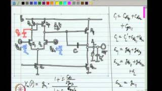
Analog IC Design by Dr. Nagendra Krishnapura, Department of Electronics & Communication Engineering, IIT Madras. For more details on NPTEL visit http://nptel.iitm.ac.in
Analog IC Design by Dr. Nagendra Krishnapura, Department of Electronics & Communication Engineering, IIT Madras. For more details on NPTEL visit http://nptel.iitm.ac.in
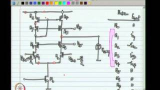
Analog IC Design by Dr. Nagendra Krishnapura, Department of Electronics & Communication Engineering, IIT Madras. For more details on NPTEL visit http://nptel.iitm.ac.in
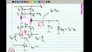
Analog IC Design by Dr. Nagendra Krishnapura, Department of Electronics & Communication Engineering, IIT Madras. For more details on NPTEL visit http://nptel.iitm.ac.in
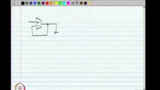
Analog IC Design by Dr. Nagendra Krishnapura, Department of Electronics & Communication Engineering, IIT Madras. For more details on NPTEL visit http://nptel.iitm.ac.in
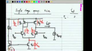
Analog IC Design by Dr. Nagendra Krishnapura, Department of Electronics & Communication Engineering, IIT Madras. For more details on NPTEL visit http://nptel.iitm.ac.in
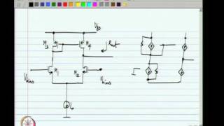
Analog IC Design by Dr. Nagendra Krishnapura, Department of Electronics & Communication Engineering, IIT Madras. For more details on NPTEL visit http://nptel.iitm.ac.in

Analog IC Design by Dr. Nagendra Krishnapura, Department of Electronics & Communication Engineering, IIT Madras. For more details on NPTEL visit http://nptel.iitm.ac.in

Analog IC Design by Dr. Nagendra Krishnapura, Department of Electronics & Communication Engineering, IIT Madras. For more details on NPTEL visit http://nptel.iitm.ac.in
Analog IC Design by Dr. Nagendra Krishnapura, Department of Electronics & Communication Engineering, IIT Madras. For more details on NPTEL visit http://nptel.iitm.ac.in

Analog IC Design by Dr. Nagendra Krishnapura, Department of Electronics & Communication Engineering, IIT Madras. For more details on NPTEL visit http://nptel.iitm.ac.in
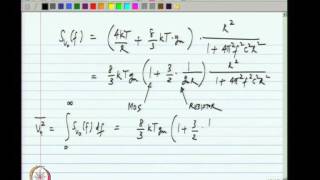
Analog IC Design by Dr. Nagendra Krishnapura, Department of Electronics & Communication Engineering, IIT Madras. For more details on NPTEL visit http://nptel.iitm.ac.in

Analog IC Design by Dr. Nagendra Krishnapura, Department of Electronics & Communication Engineering, IIT Madras. For more details on NPTEL visit http://nptel.iitm.ac.in

Analog IC Design by Dr. Nagendra Krishnapura, Department of Electronics & Communication Engineering, IIT Madras. For more details on NPTEL visit http://nptel.iitm.ac.in

Analog IC Design by Dr. Nagendra Krishnapura, Department of Electronics & Communication Engineering, IIT Madras. For more details on NPTEL visit http://nptel.iitm.ac.in

Analog IC Design by Dr. Nagendra Krishnapura, Department of Electronics & Communication Engineering, IIT Madras. For more details on NPTEL visit http://nptel.iitm.ac.in

Analog IC Design by Dr. Nagendra Krishnapura, Department of Electronics & Communication Engineering, IIT Madras. For more details on NPTEL visit http://nptel.iitm.ac.in

Analog IC Design by Dr. Nagendra Krishnapura, Department of Electronics & Communication Engineering, IIT Madras. For more details on NPTEL visit http://nptel.iitm.ac.in
Analog IC Design by Dr. Nagendra Krishnapura, Department of Electronics & Communication Engineering, IIT Madras. For more details on NPTEL visit http://nptel.iitm.ac.in

Analog IC Design by Dr. Nagendra Krishnapura, Department of Electronics & Communication Engineering, IIT Madras. For more details on NPTEL visit http://nptel.iitm.ac.in
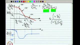
Analog IC Design by Dr. Nagendra Krishnapura, Department of Electronics & Communication Engineering, IIT Madras. For more details on NPTEL visit http://nptel.iitm.ac.in

Analog IC Design by Dr. Nagendra Krishnapura, Department of Electronics & Communication Engineering, IIT Madras. For more details on NPTEL visit http://nptel.iitm.ac.in

Analog IC Design by Dr. Nagendra Krishnapura, Department of Electronics & Communication Engineering, IIT Madras. For more details on NPTEL visit http://nptel.iitm.ac.in

Analog IC Design by Dr. Nagendra Krishnapura, Department of Electronics & Communication Engineering, IIT Madras. For more details on NPTEL visit http://nptel.iitm.ac.in
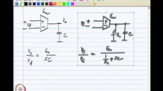
Analog IC Design by Dr. Nagendra Krishnapura, Department of Electronics & Communication Engineering, IIT Madras. For more details on NPTEL visit http://nptel.iitm.ac.in

Analog IC Design by Dr. Nagendra Krishnapura, Department of Electronics & Communication Engineering, IIT Madras. For more details on NPTEL visit http://nptel.iitm.ac.in

Analog IC Design by Dr. Nagendra Krishnapura, Department of Electronics & Communication Engineering, IIT Madras. For more details on NPTEL visit http://nptel.iitm.ac.in
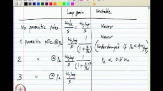
Analog IC Design by Dr. Nagendra Krishnapura, Department of Electronics & Communication Engineering, IIT Madras. For more details on NPTEL visit http://nptel.iitm.ac.in

Analog IC Design by Dr. Nagendra Krishnapura, Department of Electronics & Communication Engineering, IIT Madras. For more details on NPTEL visit http://nptel.iitm.ac.in
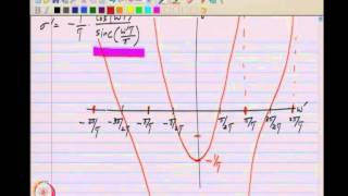
Analog IC Design by Dr. Nagendra Krishnapura, Department of Electronics & Communication Engineering, IIT Madras. For more details on NPTEL visit http://nptel.iitm.ac.in
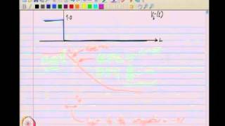
Analog IC Design by Dr. Nagendra Krishnapura, Department of Electronics & Communication Engineering, IIT Madras. For more details on NPTEL visit http://nptel.iitm.ac.in

Analog IC Design by Dr. Nagendra Krishnapura, Department of Electronics & Communication Engineering, IIT Madras. For more details on NPTEL visit http://nptel.iitm.ac.in
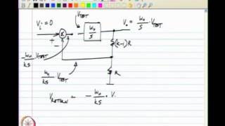
Analog IC Design by Dr. Nagendra Krishnapura, Department of Electronics & Communication Engineering, IIT Madras. For more details on NPTEL visit http://nptel.iitm.ac.in
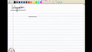
Analog IC Design by Dr. Nagendra Krishnapura, Department of Electronics & Communication Engineering, IIT Madras. For more details on NPTEL visit http://nptel.iitm.ac.in
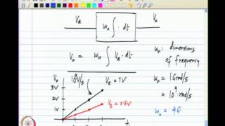
Analog IC Design by Dr. Nagendra Krishnapura, Department of Electronics & Communication Engineering, IIT Madras. For more details on NPTEL visit http://nptel.iitm.ac.in

Analog IC Design by Dr. Nagendra Krishnapura, Department of Electronics & Communication Engineering, IIT Madras. For more details on NPTEL visit http://nptel.iitm.ac.in
Ship Resistance and Propulsion by Prof. V. Anantha Subramanian,Dr. P. Krishnankutty, Department of Ocean Engineering, IITMadras. For more details on NPTEL visit http://nptel.iitm.ac.in
Semiconductor Device Modeling by Prof. S. Karmalkar,Department of Electrical Engineering,IIT Madras.For more details on NPTEL visit http://nptel.iitm.ac.in

Semiconductor Device Modeling by Prof. S. Karmalkar,Department of Electrical Engineering,IIT Madras.For more details on NPTEL visit http://nptel.iitm.ac.in

Semiconductor Device Modeling by Prof. S. Karmalkar,Department of Electrical Engineering,IIT Madras.For more details on NPTEL visit http://nptel.iitm.ac.in

Semiconductor Device Modeling by Prof. S. Karmalkar,Department of Electrical Engineering,IIT Madras.For more details on NPTEL visit http://nptel.iitm.ac.in

Semiconductor Device Modeling by Prof. S. Karmalkar,Department of Electrical Engineering,IIT Madras.For more details on NPTEL visit http://nptel.iitm.ac.in

Semiconductor Device Modeling by Prof. S. Karmalkar,Department of Electrical Engineering,IIT Madras.For more details on NPTEL visit http://nptel.iitm.ac.in
Semiconductor Device Modeling by Prof. S. Karmalkar,Department of Electrical Engineering,IIT Madras.For more details on NPTEL visit http://nptel.iitm.ac.in
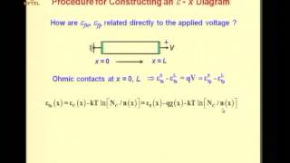
Semiconductor Device Modeling by Prof. S. Karmalkar,Department of Electrical Engineering,IIT Madras.For more details on NPTEL visit http://nptel.iitm.ac.in
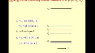
Semiconductor Device Modeling by Prof. S. Karmalkar,Department of Electrical Engineering,IIT Madras.For more details on NPTEL visit http://nptel.iitm.ac.in

Semiconductor Device Modeling by Prof. S. Karmalkar,Department of Electrical Engineering,IIT Madras.For more details on NPTEL visit http://nptel.iitm.ac.in

Semiconductor Device Modeling by Prof. S. Karmalkar,Department of Electrical Engineering,IIT Madras.For more details on NPTEL visit http://nptel.iitm.ac.in
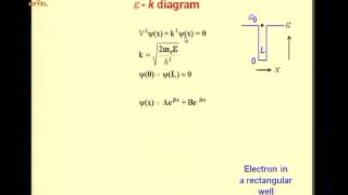
Semiconductor Device Modeling by Prof. S. Karmalkar,Department of Electrical Engineering,IIT Madras.For more details on NPTEL visit http://nptel.iitm.ac.in
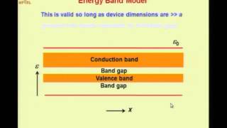
Semiconductor Device Modeling by Prof. S. Karmalkar,Department of Electrical Engineering,IIT Madras.For more details on NPTEL visit http://nptel.iitm.ac.in

Semiconductor Device Modeling by Prof. S. Karmalkar,Department of Electrical Engineering,IIT Madras.For more details on NPTEL visit http://nptel.iitm.ac.in
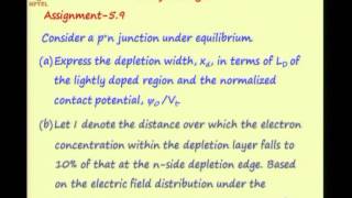
Semiconductor Device Modeling by Prof. S. Karmalkar,Department of Electrical Engineering,IIT Madras.For more details on NPTEL visit http://nptel.iitm.ac.in
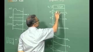
Semiconductor Device Modeling by Prof. S. Karmalkar,Department of Electrical Engineering,IIT Madras.For more details on NPTEL visit http://nptel.iitm.ac.in

Semiconductor Device Modeling by Prof. S. Karmalkar,Department of Electrical Engineering,IIT Madras.For more details on NPTEL visit http://nptel.iitm.ac.in

Semiconductor Device Modeling by Prof. S. Karmalkar,Department of Electrical Engineering,IIT Madras.For more details on NPTEL visit http://nptel.iitm.ac.in

Semiconductor Device Modeling by Prof. S. Karmalkar,Department of Electrical Engineering,IIT Madras.For more details on NPTEL visit http://nptel.iitm.ac.in
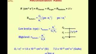
Semiconductor Device Modeling by Prof. S. Karmalkar,Department of Electrical Engineering,IIT Madras.For more details on NPTEL visit http://nptel.iitm.ac.in

Semiconductor Device Modeling by Prof. S. Karmalkar,Department of Electrical Engineering,IIT Madras.For more details on NPTEL visit http://nptel.iitm.ac.in
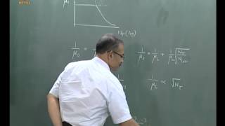
Semiconductor Device Modeling by Prof. S. Karmalkar,Department of Electrical Engineering,IIT Madras.For more details on NPTEL visit http://nptel.iitm.ac.in
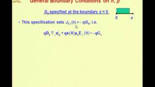
Semiconductor Device Modeling by Prof. S. Karmalkar,Department of Electrical Engineering,IIT Madras.For more details on NPTEL visit http://nptel.iitm.ac.in

Semiconductor Device Modeling by Prof. S. Karmalkar,Department of Electrical Engineering,IIT Madras.For more details on NPTEL visit http://nptel.iitm.ac.in
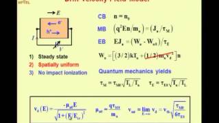
Semiconductor Device Modeling by Prof. S. Karmalkar,Department of Electrical Engineering,IIT Madras.For more details on NPTEL visit http://nptel.iitm.ac.in

Semiconductor Device Modeling by Prof. S. Karmalkar,Department of Electrical Engineering,IIT Madras.For more details on NPTEL visit http://nptel.iitm.ac.in

Semiconductor Device Modeling by Prof. S. Karmalkar,Department of Electrical Engineering,IIT Madras.For more details on NPTEL visit http://nptel.iitm.ac.in

Semiconductor Device Modeling by Prof. S. Karmalkar,Department of Electrical Engineering,IIT Madras.For more details on NPTEL visit http://nptel.iitm.ac.in
Semiconductor Device Modeling by Prof. S. Karmalkar,Department of Electrical Engineering,IIT Madras.For more details on NPTEL visit http://nptel.iitm.ac.in
Semiconductor Device Modeling by Prof. S. Karmalkar,Department of Electrical Engineering,IIT Madras.For more details on NPTEL visit http://nptel.iitm.ac.in
Semiconductor Device Modeling by Prof. S. Karmalkar,Department of Electrical Engineering,IIT Madras.For more details on NPTEL visit http://nptel.iitm.ac.in

Semiconductor Device Modeling by Prof. S. Karmalkar,Department of Electrical Engineering,IIT Madras.For more details on NPTEL visit http://nptel.iitm.ac.in

Semiconductor Device Modeling by Prof. S. Karmalkar,Department of Electrical Engineering,IIT Madras.For more details on NPTEL visit http://nptel.iitm.ac.in
Semiconductor Device Modeling by Prof. S. Karmalkar,Department of Electrical Engineering,IIT Madras.For more details on NPTEL visit http://nptel.iitm.ac.in

Semiconductor Device Modeling by Prof. S. Karmalkar,Department of Electrical Engineering,IIT Madras.For more details on NPTEL visit http://nptel.iitm.ac.in

Semiconductor Device Modeling by Prof. S. Karmalkar,Department of Electrical Engineering,IIT Madras.For more details on NPTEL visit http://nptel.iitm.ac.in
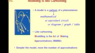
Semiconductor Device Modeling by Prof. S. Karmalkar,Department of Electrical Engineering,IIT Madras.For more details on NPTEL visit http://nptel.iitm.ac.in

Semiconductor Device Modeling by Prof. S. Karmalkar,Department of Electrical Engineering,IIT Madras.For more details on NPTEL visit http://nptel.iitm.ac.in
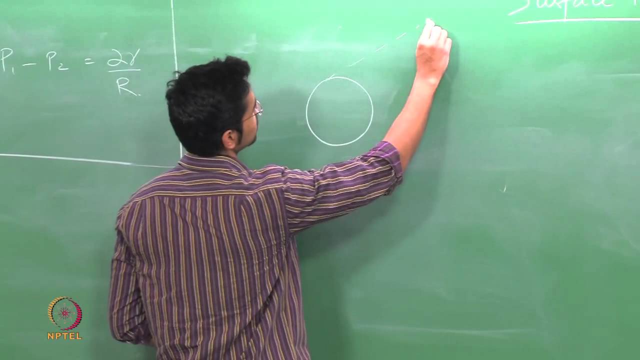
Multiphase flows:Analytical solutions and Stability Analysis by Prof. S.Pushpavanam,Department of Chemical Engineering,IIT Madras.For more details on NPTEL visit http://nptel.ac.in

Probability Foundation for Electrical Engineers by Dr. Krishna Jagannathan,Department of Electrical Engineering,IIT Madras.For more details on NPTEL visit http://nptel.ac.in
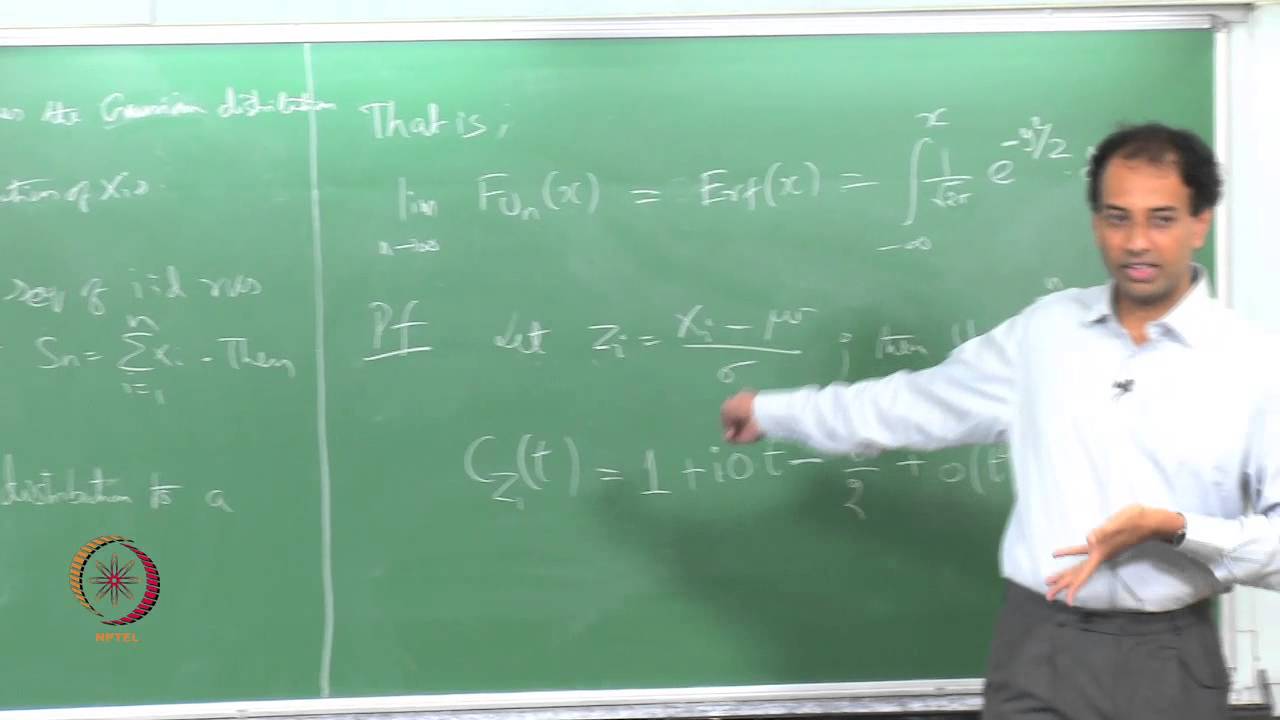
Probability Foundation for Electrical Engineers by Dr. Krishna Jagannathan,Department of Electrical Engineering,IIT Madras.For more details on NPTEL visit http://nptel.ac.in

Probability Foundation for Electrical Engineers by Dr. Krishna Jagannathan,Department of Electrical Engineering,IIT Madras.For more details on NPTEL visit http://nptel.ac.in

Probability Foundation for Electrical Engineers by Dr. Krishna Jagannathan,Department of Electrical Engineering,IIT Madras.For more details on NPTEL visit http://nptel.ac.in

Probability Foundation for Electrical Engineers by Dr. Krishna Jagannathan,Department of Electrical Engineering,IIT Madras.For more details on NPTEL visit http://nptel.ac.in
Probability Foundation for Electrical Engineers by Dr. Krishna Jagannathan,Department of Electrical Engineering,IIT Madras.For more details on NPTEL visit http://nptel.ac.in

Probability Foundation for Electrical Engineers by Dr. Krishna Jagannathan,Department of Electrical Engineering,IIT Madras.For more details on NPTEL visit http://nptel.ac.in

Probability Foundation for Electrical Engineers by Dr. Krishna Jagannathan,Department of Electrical Engineering,IIT Madras.For more details on NPTEL visit http://nptel.ac.in

Probability Foundation for Electrical Engineers by Dr. Krishna Jagannathan,Department of Electrical Engineering,IIT Madras.For more details on NPTEL visit http://nptel.ac.in

Probability Foundation for Electrical Engineers by Dr. Krishna Jagannathan,Department of Electrical Engineering,IIT Madras.For more details on NPTEL visit http://nptel.ac.in
Probability Foundation for Electrical Engineers by Dr. Krishna Jagannathan,Department of Electrical Engineering,IIT Madras.For more details on NPTEL visit http://nptel.ac.in

Probability Foundation for Electrical Engineers by Dr. Krishna Jagannathan,Department of Electrical Engineering,IIT Madras.For more details on NPTEL visit http://nptel.ac.in

Probability Foundation for Electrical Engineers by Dr. Krishna Jagannathan,Department of Electrical Engineering,IIT Madras.For more details on NPTEL visit http://nptel.ac.in
Probability Foundation for Electrical Engineers by Dr. Krishna Jagannathan,Department of Electrical Engineering,IIT Madras.For more details on NPTEL visit http://nptel.ac.in
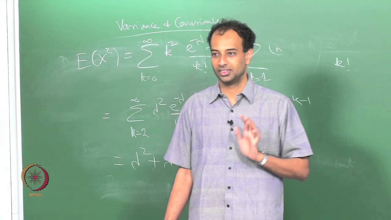
Probability Foundation for Electrical Engineers by Dr. Krishna Jagannathan,Department of Electrical Engineering,IIT Madras.For more details on NPTEL visit http://nptel.ac.in
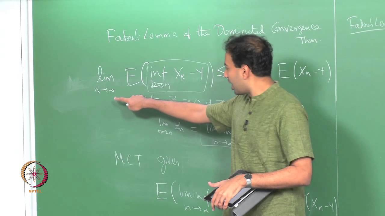
Probability Foundation for Electrical Engineers by Dr. Krishna Jagannathan,Department of Electrical Engineering,IIT Madras.For more details on NPTEL visit http://nptel.ac.in

Probability Foundation for Electrical Engineers by Dr. Krishna Jagannathan,Department of Electrical Engineering,IIT Madras.For more details on NPTEL visit http://nptel.ac.in

Probability Foundation for Electrical Engineers by Dr. Krishna Jagannathan,Department of Electrical Engineering,IIT Madras.For more details on NPTEL visit http://nptel.ac.in

Probability Foundation for Electrical Engineers by Dr. Krishna Jagannathan,Department of Electrical Engineering,IIT Madras.For more details on NPTEL visit http://nptel.ac.in

Probability Foundation for Electrical Engineers by Dr. Krishna Jagannathan,Department of Electrical Engineering,IIT Madras.For more details on NPTEL visit http://nptel.ac.in
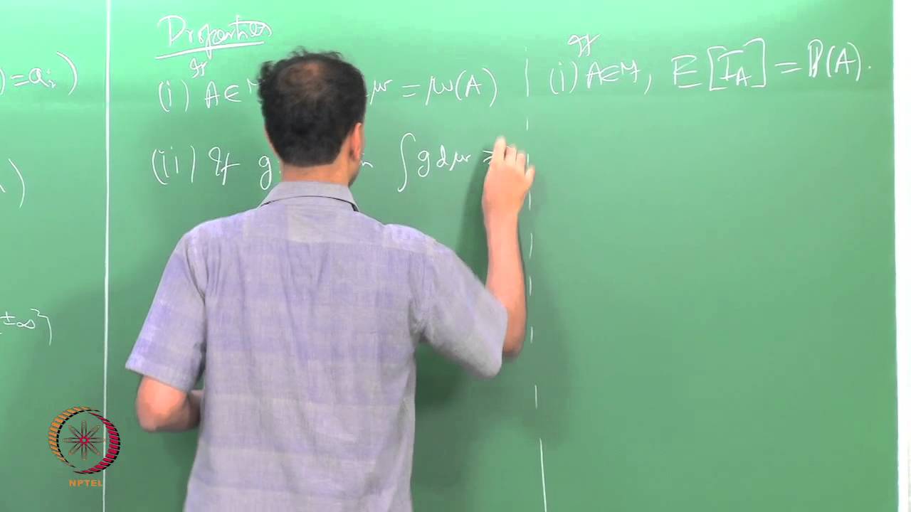
Probability Foundation for Electrical Engineers by Dr. Krishna Jagannathan,Department of Electrical Engineering,IIT Madras.For more details on NPTEL visit http://nptel.ac.in

Probability Foundation for Electrical Engineers by Dr. Krishna Jagannathan,Department of Electrical Engineering,IIT Madras.For more details on NPTEL visit http://nptel.ac.in

Probability Foundation for Electrical Engineers by Dr. Krishna Jagannathan,Department of Electrical Engineering,IIT Madras.For more details on NPTEL visit http://nptel.ac.in

Probability Foundation for Electrical Engineers by Dr. Krishna Jagannathan,Department of Electrical Engineering,IIT Madras.For more details on NPTEL visit http://nptel.ac.in
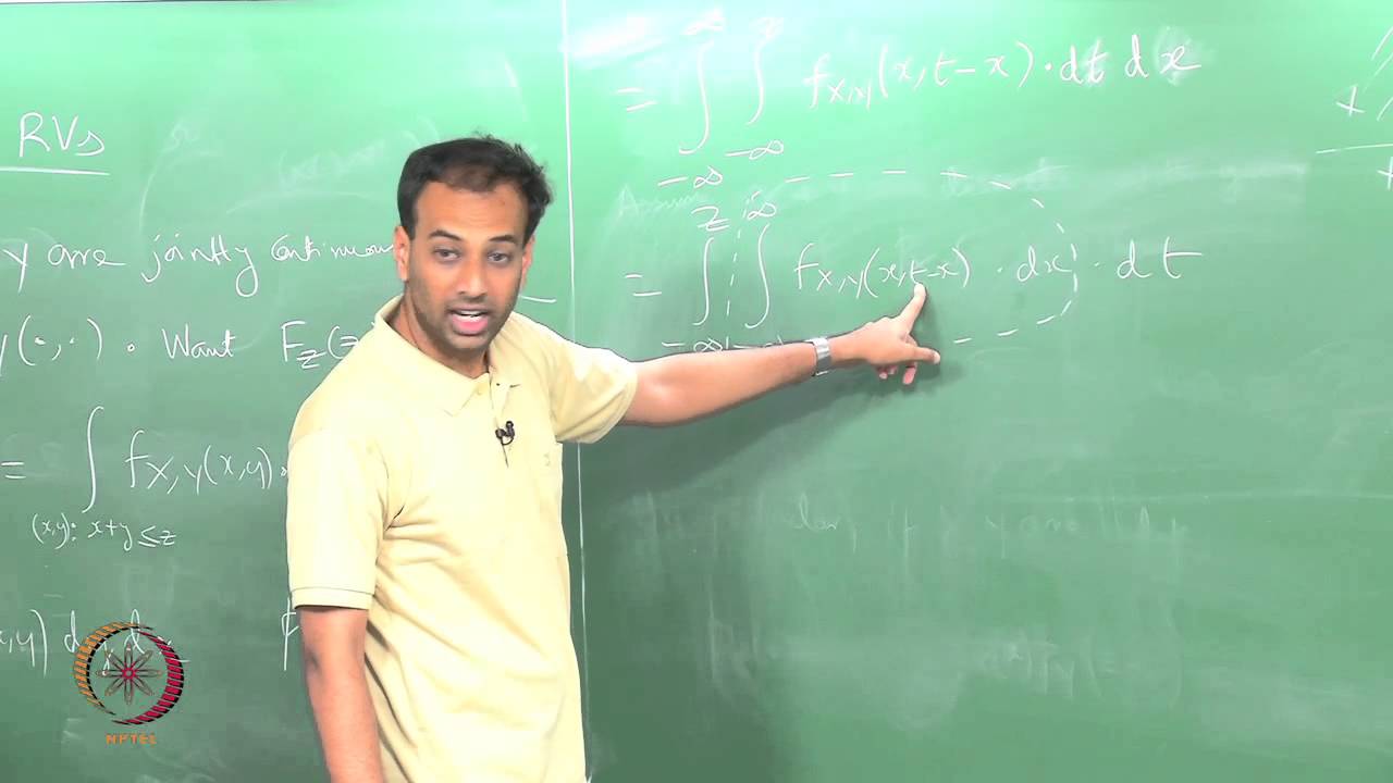
Probability Foundation for Electrical Engineers by Dr. Krishna Jagannathan,Department of Electrical Engineering,IIT Madras.For more details on NPTEL visit http://nptel.ac.in

Probability Foundation for Electrical Engineers by Dr. Krishna Jagannathan,Department of Electrical Engineering,IIT Madras.For more details on NPTEL visit http://nptel.ac.in

Probability Foundation for Electrical Engineers by Dr. Krishna Jagannathan,Department of Electrical Engineering,IIT Madras.For more details on NPTEL visit http://nptel.ac.in

Probability Foundation for Electrical Engineers by Dr. Krishna Jagannathan,Department of Electrical Engineering,IIT Madras.For more details on NPTEL visit http://nptel.ac.in

Probability Foundation for Electrical Engineers by Dr. Krishna Jagannathan,Department of Electrical Engineering,IIT Madras.For more details on NPTEL visit http://nptel.ac.in

Probability Foundation for Electrical Engineers by Dr. Krishna Jagannathan,Department of Electrical Engineering,IIT Madras.For more details on NPTEL visit http://nptel.ac.in
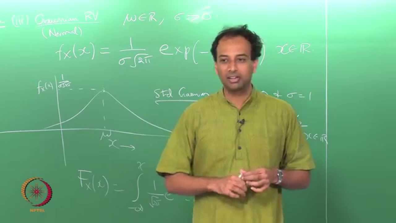
Probability Foundation for Electrical Engineers by Dr. Krishna Jagannathan,Department of Electrical Engineering,IIT Madras.For more details on NPTEL visit http://nptel.ac.in

Probability Foundation for Electrical Engineers by Dr. Krishna Jagannathan,Department of Electrical Engineering,IIT Madras.For more details on NPTEL visit http://nptel.ac.in

Probability Foundation for Electrical Engineers by Dr. Krishna Jagannathan,Department of Electrical Engineering,IIT Madras.For more details on NPTEL visit http://nptel.ac.in
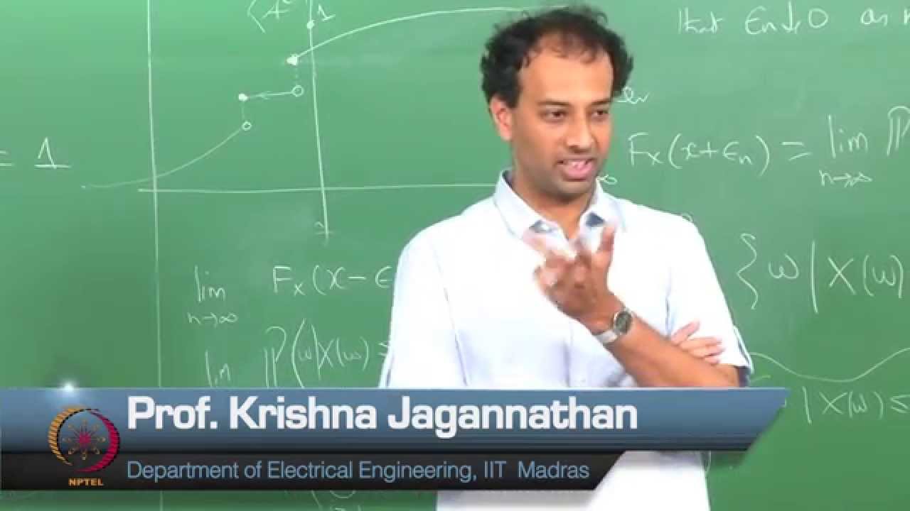
Probability Foundation for Electrical Engineers by Dr. Krishna Jagannathan,Department of Electrical Engineering,IIT Madras.For more details on NPTEL visit http://nptel.ac.in

Probability Foundation for Electrical Engineers by Dr. Krishna Jagannathan,Department of Electrical Engineering,IIT Madras.For more details on NPTEL visit http://nptel.ac.in

Probability Foundation for Electrical Engineers by Dr. Krishna Jagannathan,Department of Electrical Engineering,IIT Madras.For more details on NPTEL visit http://nptel.ac.in

Probability Foundation for Electrical Engineers by Dr. Krishna Jagannathan,Department of Electrical Engineering,IIT Madras.For more details on NPTEL visit http://nptel.ac.in
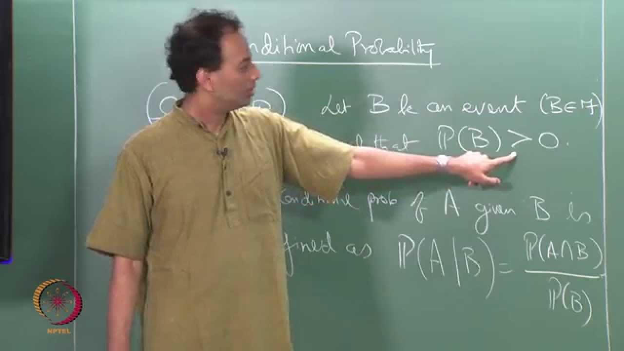
Probability Foundation for Electrical Engineers by Dr. Krishna Jagannathan,Department of Electrical Engineering,IIT Madras.For more details on NPTEL visit http://nptel.ac.in

Probability Foundation for Electrical Engineers by Dr. Krishna Jagannathan,Department of Electrical Engineering,IIT Madras.For more details on NPTEL visit http://nptel.ac.in
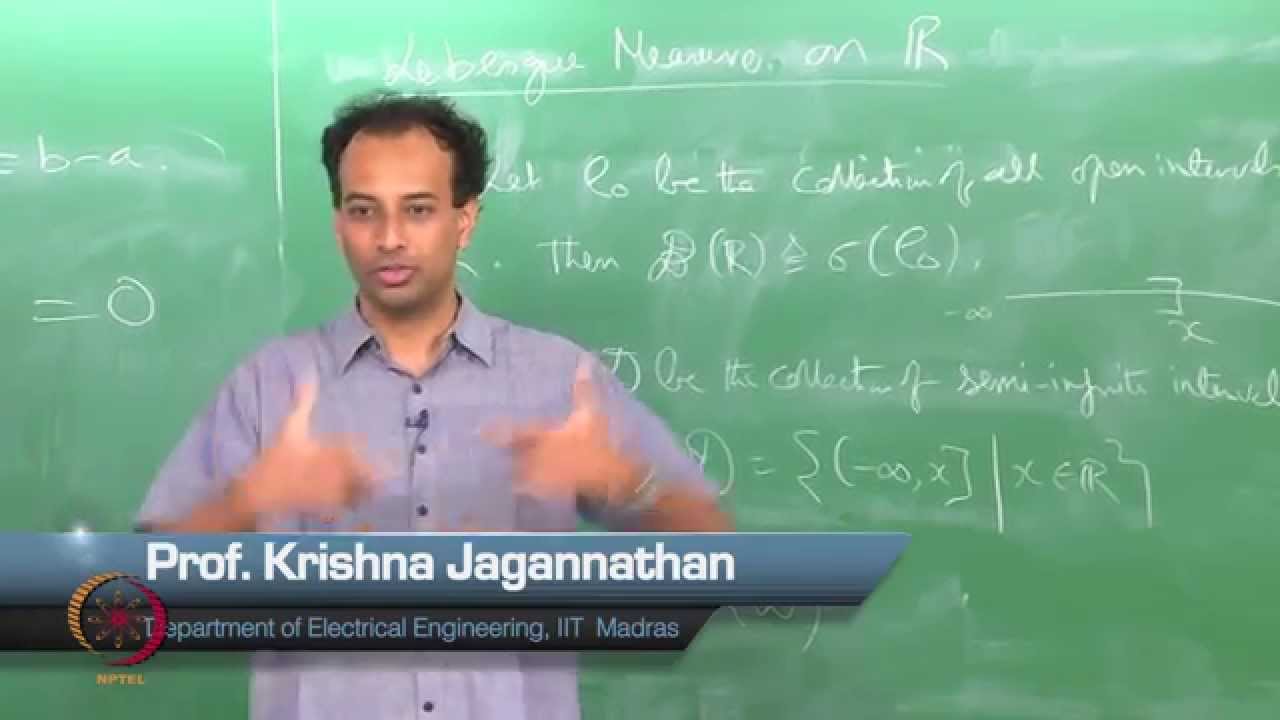
Probability Foundation for Electrical Engineers by Dr. Krishna Jagannathan,Department of Electrical Engineering,IIT Madras.For more details on NPTEL visit http://nptel.ac.in

Probability Foundation for Electrical Engineers by Dr. Krishna Jagannathan,Department of Electrical Engineering,IIT Madras.For more details on NPTEL visit http://nptel.ac.in

Probability Foundation for Electrical Engineers by Dr. Krishna Jagannathan,Department of Electrical Engineering,IIT Madras.For more details on NPTEL visit http://nptel.ac.in

Probability Foundation for Electrical Engineers by Dr. Krishna Jagannathan,Department of Electrical Engineering,IIT Madras.For more details on NPTEL visit http://nptel.ac.in

Probability Foundation for Electrical Engineers by Dr. Krishna Jagannathan,Department of Electrical Engineering,IIT Madras.For more details on NPTEL visit http://nptel.ac.in

Probability Foundation for Electrical Engineers by Dr. Krishna Jagannathan,Department of Electrical Engineering,IIT Madras.For more details on NPTEL visit http://nptel.ac.in
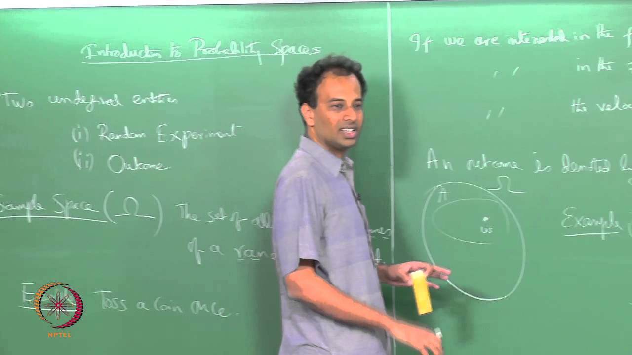
Probability Foundation for Electrical Engineers by Dr. Krishna Jagannathan,Department of Electrical Engineering,IIT Madras.For more details on NPTEL visit http://nptel.ac.in
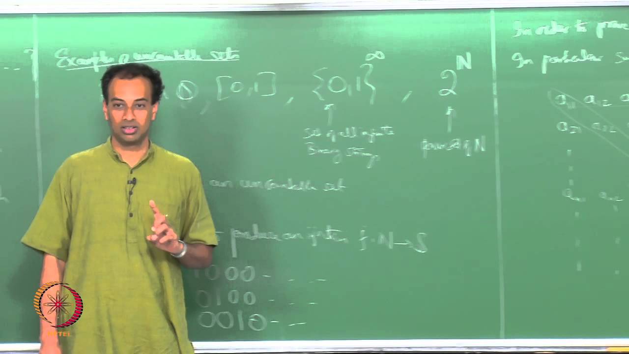
Probability Foundation for Electrical Engineers by Dr. Krishna Jagannathan,Department of Electrical Engineering,IIT Madras.For more details on NPTEL visit http://nptel.ac.in
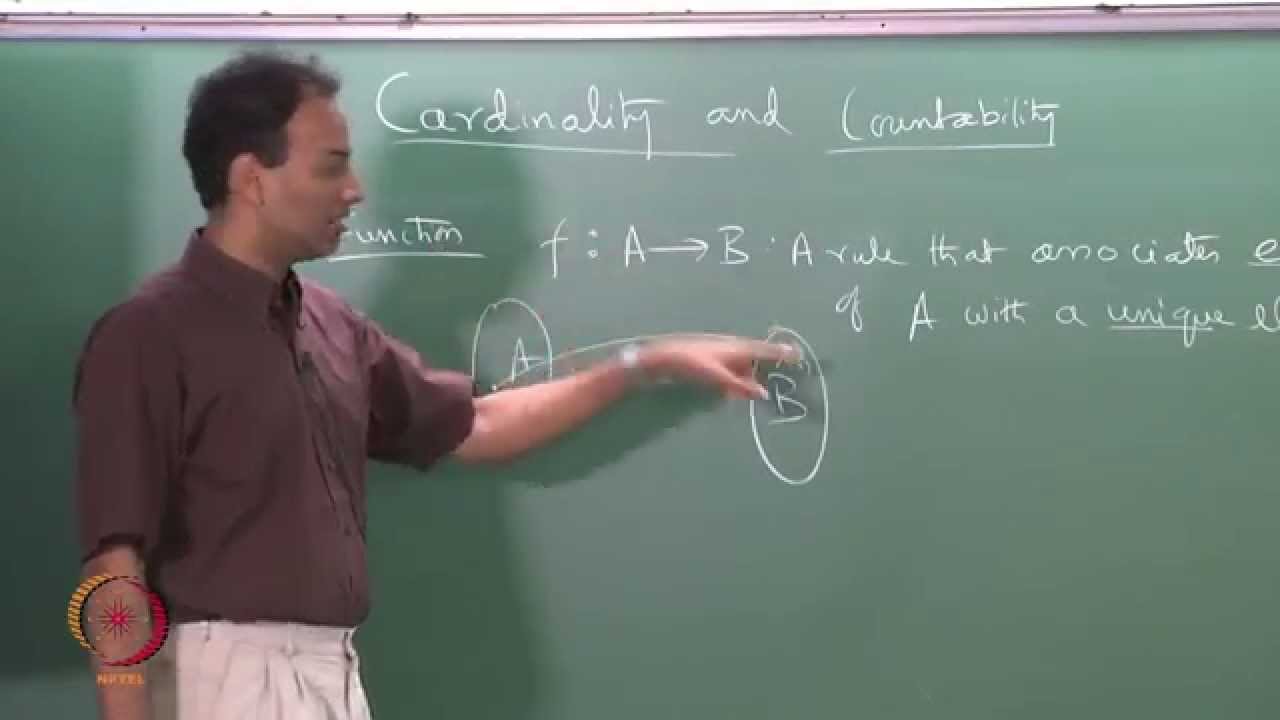
Probability Foundation for Electrical Engineers by Dr. Krishna Jagannathan,Department of Electrical Engineering,IIT Madras.For more details on NPTEL visit http://nptel.ac.in
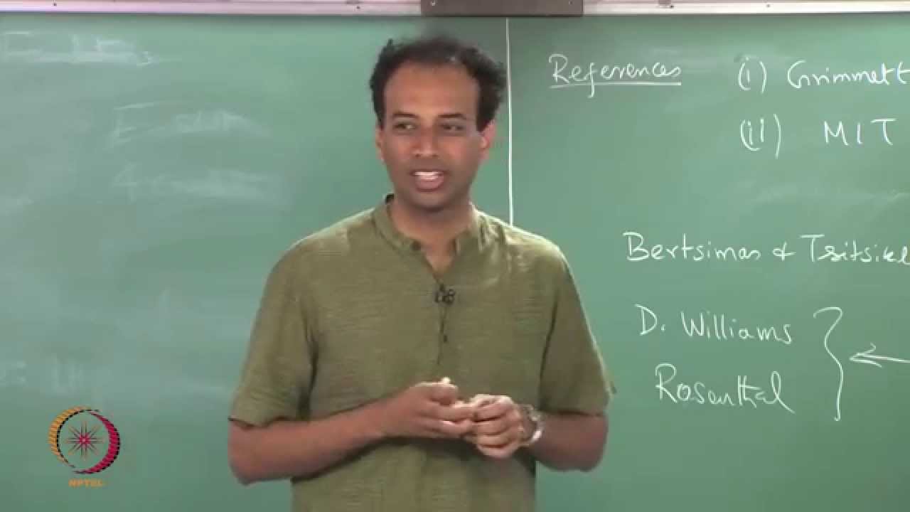
Probability Foundation for Electrical Engineers by Dr. Krishna Jagannathan,Department of Electrical Engineering,IIT Madras.For more details on NPTEL visit http://nptel.ac.in
VLSI
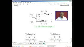
Lecture Series on VLSI Design by Prof S.Srinivasan,
Dept of Electrical Engineering, IIT Madras
For more details on NPTEl visit http://nptel.iitm.ac.in

Lecture Series on VLSI Design by Prof S.Srinivasan,
Dept of Electrical Engineering, IIT Madras
For more details on NPTEl visit http://nptel.iitm.ac.in
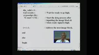
Lecture Series on VLSI Design by Prof S.Srinivasan,
Dept of Electrical Engineering, IIT Madras
For more details on NPTEl visit http://nptel.iitm.ac.in

Lecture Series on VLSI Design by Prof S.Srinivasan,
Dept of Electrical Engineering, IIT Madras
For more details on NPTEl visit http://nptel.iitm.ac.in
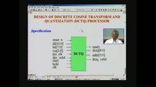
Lecture Series on VLSI Design by Prof S.Srinivasan,
Dept of Electrical Engineering, IIT Madras
For more details on NPTEl visit http://nptel.iitm.ac.in
Lecture Series on VLSI Design by Prof S.Srinivasan,
Dept of Electrical Engineering, IIT Madras
For more details on NPTEl visit http://nptel.iitm.ac.in
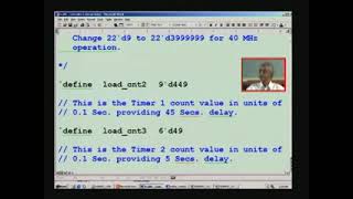
Lecture Series on VLSI Design by Prof S.Srinivasan,
Dept of Electrical Engineering, IIT Madras
For more details on NPTEl visit http://nptel.iitm.ac.in
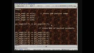
Lecture Series on VLSI Design by Prof S.Srinivasan,
Dept of Electrical Engineering, IIT Madras
For more details on NPTEl visit http://nptel.iitm.ac.in

Lecture Series on VLSI Design by Prof S.Srinivasan,
Dept of Electrical Engineering, IIT Madras
For more details on NPTEl visit http://nptel.iitm.ac.in

Lecture Series on VLSI Design by Prof S.Srinivasan,
Dept of Electrical Engineering, IIT Madras
For more details on NPTEl visit http://nptel.iitm.ac.in
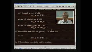
Lecture Series on VLSI Design by Prof S.Srinivasan,
Dept of Electrical Engineering, IIT Madras
For more details on NPTEl visit http://nptel.iitm.ac.in
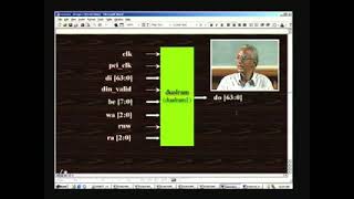
Lecture Series on VLSI Design by Prof S.Srinivasan,
Dept of Electrical Engineering, IIT Madras
For more details on NPTEl visit http://nptel.iitm.ac.in

Lecture Series on VLSI Design by Prof S.Srinivasan,
Dept of Electrical Engineering, IIT Madras
For more details on NPTEl visit http://nptel.iitm.ac.in
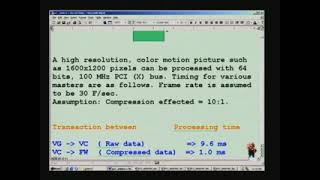
Lecture Series on VLSI Design by Prof S.Srinivasan,
Dept of Electrical Engineering, IIT Madras
For more details on NPTEl visit http://nptel.iitm.ac.in

Lecture Series on VLSI Design by Prof S.Srinivasan,
Dept of Electrical Engineering, IIT Madras
For more details on NPTEl visit http://nptel.iitm.ac.in
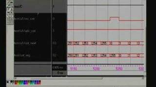
Lecture Series on VLSI Design by Prof S.Srinivasan,
Dept of Electrical Engineering, IIT Madras
For more details on NPTEl visit http://nptel.iitm.ac.in

Lecture Series on VLSI Design by Prof S.Srinivasan,
Dept of Electrical Engineering, IIT Madras
For more details on NPTEl visit http://nptel.iitm.ac.in

Lecture Series on VLSI Design by Prof S.Srinivasan,
Dept of Electrical Engineering, IIT Madras
For more details on NPTEl visit http://nptel.iitm.ac.in

Lecture Series on VLSI Design by Prof S.Srinivasan,
Dept of Electrical Engineering, IIT Madras
For more details on NPTEl visit http://nptel.iitm.ac.in

Lecture Series on VLSI Design by Prof S.Srinivasan,
Dept of Electrical Engineering, IIT Madras
For more details on NPTEl visit http://nptel.iitm.ac.in

Lecture Series on VLSI Design by Prof S.Srinivasan,
Dept of Electrical Engineering, IIT Madras
For more details on NPTEl visit http://nptel.iitm.ac.in
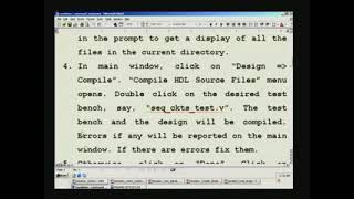
Lecture Series on VLSI Design by Prof S.Srinivasan,
Dept of Electrical Engineering, IIT Madras
For more details on NPTEl visit http://nptel.iitm.ac.in

Lecture Series on VLSI Design by Prof S.Srinivasan,
Dept of Electrical Engineering, IIT Madras
For more details on NPTEl visit http://nptel.iitm.ac.in

Lecture Series on VLSI Design by Prof S.Srinivasan,
Dept of Electrical Engineering, IIT Madras
For more details on NPTEl visit http://nptel.iitm.ac.in
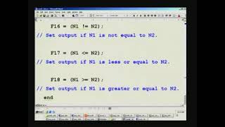
Lecture Series on VLSI Design by Prof S.Srinivasan,
Dept of Electrical Engineering, IIT Madras
For more details on NPTEl visit http://nptel.iitm.ac.in
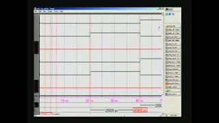
Lecture Series on VLSI Design by Prof S.Srinivasan,
Dept of Electrical Engineering, IIT Madras
For more details on NPTEl visit http://nptel.iitm.ac.in
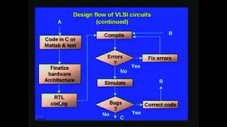
Lecture Series on VLSI Design by Prof S.Srinivasan,
Dept of Electrical Engineering, IIT Madras
For more details on NPTEl visit http://nptel.iitm.ac.in
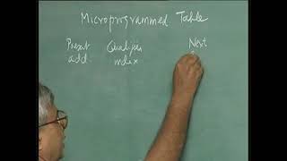
Lecture Series on VLSI Design by Prof S.Srinivasan,
Dept of Electrical Engineering, IIT Madras
For more details on NPTEl visit http://nptel.iitm.ac.in
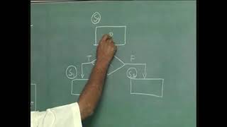
Lecture Series on VLSI Design by Prof S.Srinivasan,
Dept of Electrical Engineering, IIT Madras
For more details on NPTEl visit http://nptel.iitm.ac.in
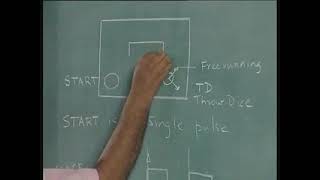
Lecture Series on VLSI Design by Prof S.Srinivasan,
Dept of Electrical Engineering, IIT Madras
For more details on NPTEl visit http://nptel.iitm.ac.in

Lecture Series on VLSI Design by Prof S.Srinivasan,
Dept of Electrical Engineering, IIT Madras
For more details on NPTEl visit http://nptel.iitm.ac.in
Lecture Series on VLSI Design by Prof S.Srinivasan,
Dept of Electrical Engineering, IIT Madras
For more details on NPTEl visit http://nptel.iitm.ac.in
Lecture Series on VLSI Design by Prof S.Srinivasan,
Dept of Electrical Engineering, IIT Madras
For more details on NPTEl visit http://nptel.iitm.ac.in
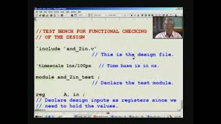
Lecture Series on VLSI Design by Prof S.Srinivasan,
Dept of Electrical Engineering, IIT Madras
For more details on NPTEl visit http://nptel.iitm.ac.in

Lecture Series on VLSI Design by Prof S.Srinivasan,
Dept of Electrical Engineering, IIT Madras
For more details on NPTEl visit http://nptel.iitm.ac.in
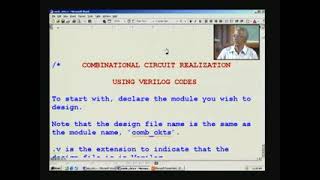
Lecture Series on VLSI Design by Prof S.Srinivasan,
Dept of Electrical Engineering, IIT Madras
For more details on NPTEl visit http://nptel.iitm.ac.in

Lecture Series on VLSI Design by Prof S.Srinivasan,
Dept of Electrical Engineering, IIT Madras
For more details on NPTEl visit http://nptel.iitm.ac.in

Lecture Series on VLSI Design by Prof S.Srinivasan,
Dept of Electrical Engineering, IIT Madras
For more details on NPTEl visit http://nptel.iitm.ac.in

Lecture Series on VLSI Design by Prof S.Srinivasan,
Dept of Electrical Engineering, IIT Madras
For more details on NPTEl visit http://nptel.iitm.ac.in

Lecture Series on VLSI Design by Prof S.Srinivasan,
Dept of Electrical Engineering, IIT Madras
For more details on NPTEl visit http://nptel.iitm.ac.in

Lecture Series on VLSI Design by Prof S.Srinivasan,
Dept of Electrical Engineering, IIT Madras
For more details on NPTEl visit http://nptel.iitm.ac.in
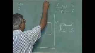
Lecture Series on VLSI Design by Prof S.Srinivasan,
Dept of Electrical Engineering, IIT Madras
For more details on NPTEl visit http://nptel.iitm.ac.in

Lecture Series on VLSI Design by Prof S.Srinivasan,
Dept of Electrical Engineering, IIT Madras
For more details on NPTEl visit http://nptel.iitm.ac.in
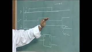
Lecture Series on VLSI Design by Prof S.Srinivasan,
Dept of Electrical Engineering, IIT Madras
For more details on NPTEl visit http://nptel.iitm.ac.in
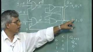
Lecture Series on VLSI Design by Prof S.Srinivasan,
Dept of Electrical Engineering, IIT Madras
For more details on NPTEl visit http://nptel.iitm.ac.in
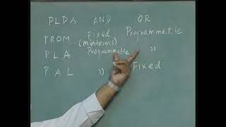
Lecture Series on VLSI Design by Prof S.Srinivasan,
Dept of Electrical Engineering, IIT Madras
For more details on NPTEl visit http://nptel.iitm.ac.in
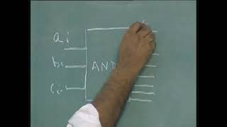
Lecture Series on VLSI Design by Prof S.Srinivasan,
Dept of Electrical Engineering, IIT Madras
For more details on NPTEl visit http://nptel.iitm.ac.in

Lecture Series on VLSI Design by Prof S.Srinivasan,
Dept of Electrical Engineering, IIT Madras
For more details on NPTEl visit http://nptel.iitm.ac.in

Lecture Series on VLSI Design by Prof S.Srinivasan,
Dept of Electrical Engineering, IIT Madras
For more details on NPTEl visit http://nptel.iitm.ac.in

Electronic materials, devices, and fabrication by Prof S. Parasuraman,Department of Metallurgy and Material Science,IIT Madras.For more details on NPTEL visit http://nptel.ac.in

Electronic materials, devices, and fabrication by Prof S. Parasuraman,Department of Metallurgy and Material Science,IIT Madras.For more details on NPTEL visit http://nptel.ac.in
Electronic materials, devices, and fabrication by Prof S. Parasuraman,Department of Metallurgy and Material Science,IIT Madras.For more details on NPTEL visit http://nptel.ac.in

Basic Electrical Circuits by Dr. Nagendra Krishnapura,Department of Electronics & Communication Engineering,IIT Madras.For more details on NPTEL visit http://nptel.ac.in

Basic Electrical Circuits by Dr. Nagendra Krishnapura,Department of Electronics & Communication Engineering,IIT Madras.For more details on NPTEL visit http://nptel.ac.in

Basic Electrical Circuits by Dr. Nagendra Krishnapura,Department of Electronics & Communication Engineering,IIT Madras.For more details on NPTEL visit http://nptel.ac.in
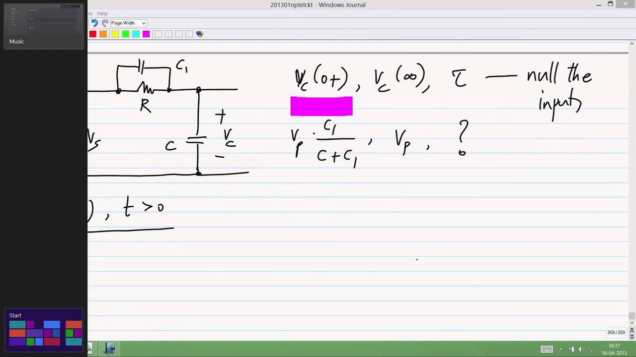
Basic Electrical Circuits by Dr. Nagendra Krishnapura,Department of Electronics & Communication Engineering,IIT Madras.For more details on NPTEL visit http://nptel.ac.in

Basic Electrical Circuits by Dr. Nagendra Krishnapura,Department of Electronics & Communication Engineering,IIT Madras.For more details on NPTEL visit http://nptel.ac.in

Basic Electrical Circuits by Dr. Nagendra Krishnapura,Department of Electronics & Communication Engineering,IIT Madras.For more details on NPTEL visit http://nptel.ac.in

Basic Electrical Circuits by Dr. Nagendra Krishnapura,Department of Electronics & Communication Engineering,IIT Madras.For more details on NPTEL visit http://nptel.ac.in

Basic Electrical Circuits by Dr. Nagendra Krishnapura,Department of Electronics & Communication Engineering,IIT Madras.For more details on NPTEL visit http://nptel.ac.in
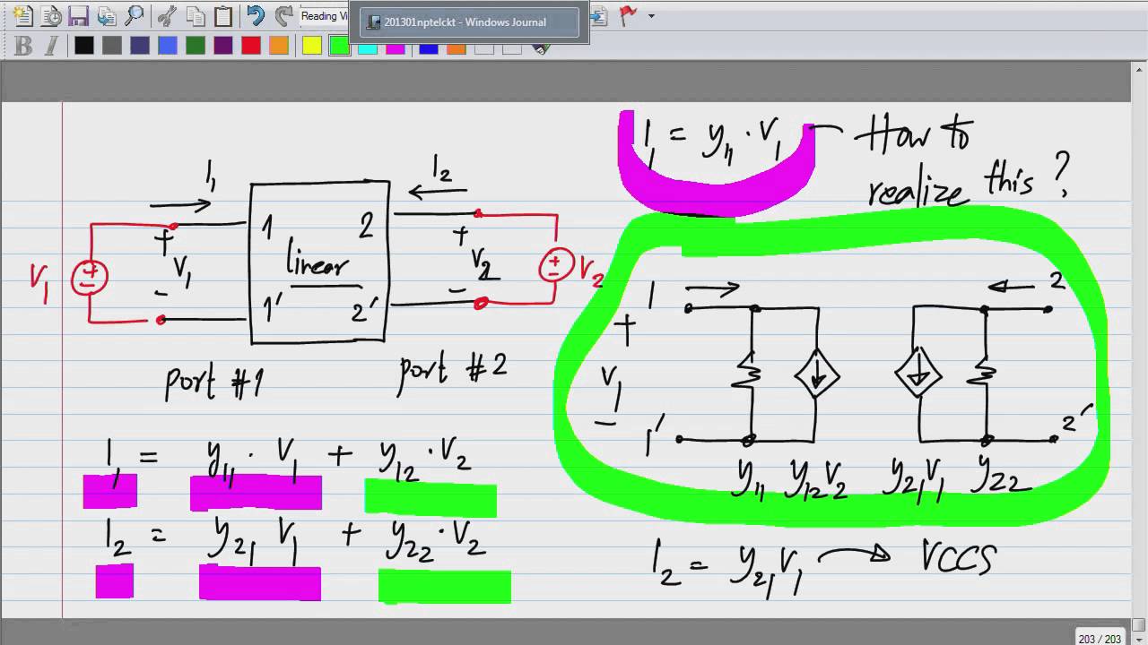
Basic Electrical Circuits by Dr. Nagendra Krishnapura,Department of Electronics & Communication Engineering,IIT Madras.For more details on NPTEL visit http://nptel.ac.in

Basic Electrical Circuits by Dr. Nagendra Krishnapura,Department of Electronics & Communication Engineering,IIT Madras.For more details on NPTEL visit http://nptel.ac.in

Basic Electrical Circuits by Dr. Nagendra Krishnapura,Department of Electronics & Communication Engineering,IIT Madras.For more details on NPTEL visit http://nptel.ac.in

Mod-01 Lec-10 Thevenin and Norton (theorem and) equivalent circuits; Power conservation in a circuit
Basic Electrical Circuits by Dr. Nagendra Krishnapura,Department of Electronics & Communication Engineering,IIT Madras.For more details on NPTEL visit http://nptel.ac.in
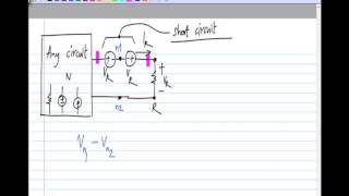
Basic Electrical Circuits by Dr. Nagendra Krishnapura,Department of Electronics & Communication Engineering,IIT Madras.For more details on NPTEL visit http://nptel.ac.in

Basic Electrical Circuits by Dr. Nagendra Krishnapura,Department of Electronics & Communication Engineering,IIT Madras.For more details on NPTEL visit http://nptel.ac.in
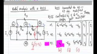
Basic Electrical Circuits by Dr. Nagendra Krishnapura,Department of Electronics & Communication Engineering,IIT Madras.For more details on NPTEL visit http://nptel.ac.in

Basic Electrical Circuits by Dr. Nagendra Krishnapura,Department of Electronics & Communication Engineering,IIT Madras.For more details on NPTEL visit http://nptel.ac.in
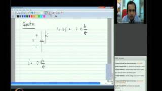
Basic Electrical Circuits by Dr. Nagendra Krishnapura,Department of Electronics & Communication Engineering,IIT Madras.For more details on NPTEL visit http://nptel.ac.in
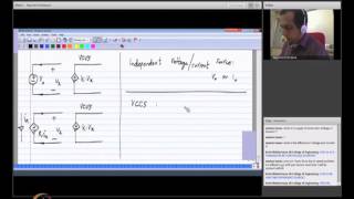
Basic Electrical Circuits by Dr. Nagendra Krishnapura,Department of Electronics & Communication Engineering,IIT Madras.For more details on NPTEL visit http://nptel.ac.in

Basic Electrical Circuits by Dr. Nagendra Krishnapura,Department of Electronics & Communication Engineering,IIT Madras.For more details on NPTEL visit http://nptel.ac.in

Basic Electrical Circuits by Dr. Nagendra Krishnapura,Department of Electronics & Communication Engineering,IIT Madras.For more details on NPTEL visit http://nptel.ac.in

Modelling and Analysis of Electric Machines by Dr. Krishna Vasudevan,Department of Electrical Engineering,IIT Madras.For more details on NPTEL visit http://nptel.ac.in
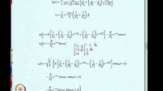
Modelling and Analysis of Electric Machines by Dr. Krishna Vasudevan,Department of Electrical Engineering,IIT Madras.For more details on NPTEL visit http://nptel.ac.in
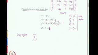
Modelling and Analysis of Electric Machines by Dr. Krishna Vasudevan,Department of Electrical Engineering,IIT Madras.For more details on NPTEL visit http://nptel.ac.in
Modelling and Analysis of Electric Machines by Dr. Krishna Vasudevan,Department of Electrical Engineering,IIT Madras.For more details on NPTEL visit http://nptel.ac.in

Modelling and Analysis of Electric Machines by Dr. Krishna Vasudevan,Department of Electrical Engineering,IIT Madras.For more details on NPTEL visit http://nptel.ac.in
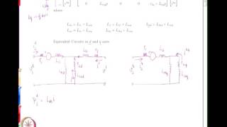
Modelling and Analysis of Electric Machines by Dr. Krishna Vasudevan,Department of Electrical Engineering,IIT Madras.For more details on NPTEL visit http://nptel.ac.in

Modelling and Analysis of Electric Machines by Dr. Krishna Vasudevan,Department of Electrical Engineering,IIT Madras.For more details on NPTEL visit http://nptel.ac.in

Modelling and Analysis of Electric Machines by Dr. Krishna Vasudevan,Department of Electrical Engineering,IIT Madras.For more details on NPTEL visit http://nptel.ac.in

Modelling and Analysis of Electric Machines by Dr. Krishna Vasudevan,Department of Electrical Engineering,IIT Madras.For more details on NPTEL visit http://nptel.ac.in
Modelling and Analysis of Electric Machines by Dr. Krishna Vasudevan,Department of Electrical Engineering,IIT Madras.For more details on NPTEL visit http://nptel.ac.in
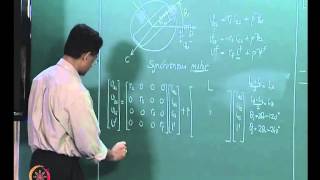
Modelling and Analysis of Electric Machines by Dr. Krishna Vasudevan,Department of Electrical Engineering,IIT Madras.For more details on NPTEL visit http://nptel.ac.in

Modelling and Analysis of Electric Machines by Dr. Krishna Vasudevan,Department of Electrical Engineering,IIT Madras.For more details on NPTEL visit http://nptel.ac.in

Modelling and Analysis of Electric Machines by Dr. Krishna Vasudevan,Department of Electrical Engineering,IIT Madras.For more details on NPTEL visit http://nptel.ac.in
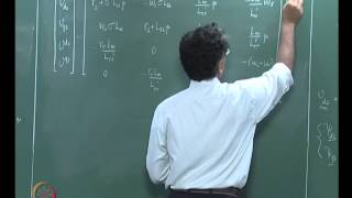
Modelling and Analysis of Electric Machines by Dr. Krishna Vasudevan,Department of Electrical Engineering,IIT Madras.For more details on NPTEL visit http://nptel.ac.in
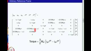
Modelling and Analysis of Electric Machines by Dr. Krishna Vasudevan,Department of Electrical Engineering,IIT Madras.For more details on NPTEL visit http://nptel.ac.in
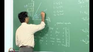
Modelling and Analysis of Electric Machines by Dr. Krishna Vasudevan,Department of Electrical Engineering,IIT Madras.For more details on NPTEL visit http://nptel.ac.in

Modelling and Analysis of Electric Machines by Dr. Krishna Vasudevan,Department of Electrical Engineering,IIT Madras.For more details on NPTEL visit http://nptel.ac.in

Modelling and Analysis of Electric Machines by Dr. Krishna Vasudevan,Department of Electrical Engineering,IIT Madras.For more details on NPTEL visit http://nptel.ac.in

Modelling and Analysis of Electric Machines by Dr. Krishna Vasudevan,Department of Electrical Engineering,IIT Madras.For more details on NPTEL visit http://nptel.ac.in
Modelling and Analysis of Electric Machines by Dr. Krishna Vasudevan,Department of Electrical Engineering,IIT Madras.For more details on NPTEL visit http://nptel.ac.in
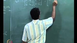
Modelling and Analysis of Electric Machines by Dr. Krishna Vasudevan,Department of Electrical Engineering,IIT Madras.For more details on NPTEL visit http://nptel.ac.in

Modelling and Analysis of Electric Machines by Dr. Krishna Vasudevan,Department of Electrical Engineering,IIT Madras.For more details on NPTEL visit http://nptel.ac.in
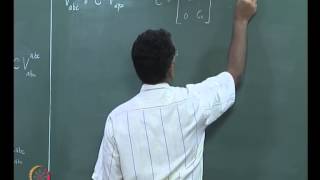
Modelling and Analysis of Electric Machines by Dr. Krishna Vasudevan,Department of Electrical Engineering,IIT Madras.For more details on NPTEL visit http://nptel.ac.in
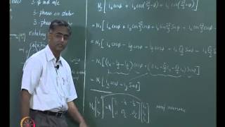
Modelling and Analysis of Electric Machines by Dr. Krishna Vasudevan,Department of Electrical Engineering,IIT Madras.For more details on NPTEL visit http://nptel.ac.in
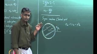
Modelling and Analysis of Electric Machines by Dr. Krishna Vasudevan,Department of Electrical Engineering,IIT Madras.For more details on NPTEL visit http://nptel.ac.in
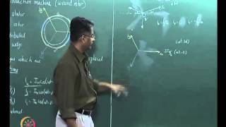
Modelling and Analysis of Electric Machines by Dr. Krishna Vasudevan,Department of Electrical Engineering,IIT Madras.For more details on NPTEL visit http://nptel.ac.in
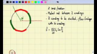
Modelling and Analysis of Electric Machines by Dr. Krishna Vasudevan,Department of Electrical Engineering,IIT Madras.For more details on NPTEL visit http://nptel.ac.in

Modelling and Analysis of Electric Machines by Dr. Krishna Vasudevan,Department of Electrical Engineering,IIT Madras.For more details on NPTEL visit http://nptel.ac.in

Modelling and Analysis of Electric Machines by Dr. Krishna Vasudevan,Department of Electrical Engineering,IIT Madras.For more details on NPTEL visit http://nptel.ac.in

Modelling and Analysis of Electric Machines by Dr. Krishna Vasudevan,Department of Electrical Engineering,IIT Madras.For more details on NPTEL visit http://nptel.ac.in

Modelling and Analysis of Electric Machines by Dr. Krishna Vasudevan,Department of Electrical Engineering,IIT Madras.For more details on NPTEL visit http://nptel.ac.in

Modelling and Analysis of Electric Machines by Dr. Krishna Vasudevan,Department of Electrical Engineering,IIT Madras.For more details on NPTEL visit http://nptel.ac.in
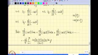
Modelling and Analysis of Electric Machines by Dr. Krishna Vasudevan,Department of Electrical Engineering,IIT Madras.For more details on NPTEL visit http://nptel.ac.in

Modelling and Analysis of Electric Machines by Dr. Krishna Vasudevan,Department of Electrical Engineering,IIT Madras.For more details on NPTEL visit http://nptel.ac.in

Modelling and Analysis of Electric Machines by Dr. Krishna Vasudevan,Department of Electrical Engineering,IIT Madras.For more details on NPTEL visit http://nptel.ac.in

Modelling and Analysis of Electric Machines by Dr. Krishna Vasudevan,Department of Electrical Engineering,IIT Madras.For more details on NPTEL visit http://nptel.ac.in

Modelling and Analysis of Electric Machines by Dr. Krishna Vasudevan,Department of Electrical Engineering,IIT Madras.For more details on NPTEL visit http://nptel.ac.in

Modelling and Analysis of Electric Machines by Dr. Krishna Vasudevan,Department of Electrical Engineering,IIT Madras.For more details on NPTEL visit http://nptel.ac.in

Modelling and Analysis of Electric Machines by Dr. Krishna Vasudevan,Department of Electrical Engineering,IIT Madras.For more details on NPTEL visit http://nptel.ac.in

Modelling and Analysis of Electric Machines by Dr. Krishna Vasudevan,Department of Electrical Engineering,IIT Madras.For more details on NPTEL visit http://nptel.ac.in

Modelling and Analysis of Electric Machines by Dr. Krishna Vasudevan,Department of Electrical Engineering,IIT Madras.For more details on NPTEL visit http://nptel.ac.in

Modelling and Analysis of Electric Machines by Dr. Krishna Vasudevan,Department of Electrical Engineering,IIT Madras.For more details on NPTEL visit http://nptel.ac.in

Digital Switching by Prof. Yatindra N Singh,Department of Electronics & Communication Engineering,IIT Kanpur.For more details on NPTEL visit http://nptel.ac.in.

Digital Switching by Prof. Yatindra N Singh,Department of Electronics & Communication Engineering,IIT Kanpur.For more details on NPTEL visit http://nptel.ac.in.

Digital Switching by Prof. Yatindra N Singh,Department of Electronics & Communication Engineering,IIT Kanpur.For more details on NPTEL visit http://nptel.ac.in.

Digital Switching by Prof. Yatindra N Singh,Department of Electronics & Communication Engineering,IIT Kanpur.For more details on NPTEL visit http://nptel.ac.in.

Digital Switching by Prof. Yatindra N Singh,Department of Electronics & Communication Engineering,IIT Kanpur.For more details on NPTEL visit http://nptel.ac.in.

Digital Switching by Prof. Yatindra N Singh,Department of Electronics & Communication Engineering,IIT Kanpur.For more details on NPTEL visit http://nptel.ac.in.

Digital Switching by Prof. Yatindra N Singh,Department of Electronics & Communication Engineering,IIT Kanpur.For more details on NPTEL visit http://nptel.ac.in.

Digital Switching by Prof. Yatindra N Singh,Department of Electronics & Communication Engineering,IIT Kanpur.For more details on NPTEL visit http://nptel.ac.in.

Digital Switching by Prof. Yatindra N Singh,Department of Electronics & Communication Engineering,IIT Kanpur.For more details on NPTEL visit http://nptel.ac.in.

Digital Switching by Prof. Yatindra N Singh,Department of Electronics & Communication Engineering,IIT Kanpur.For more details on NPTEL visit http://nptel.ac.in.

Digital Switching by Prof. Yatindra N Singh,Department of Electronics & Communication Engineering,IIT Kanpur.For more details on NPTEL visit http://nptel.ac.in.

Digital Switching by Prof. Yatindra N Singh,Department of Electronics & Communication Engineering,IIT Kanpur.For more details on NPTEL visit http://nptel.ac.in.

Digital Switching by Prof. Yatindra N Singh,Department of Electronics & Communication Engineering,IIT Kanpur.For more details on NPTEL visit http://nptel.ac.in.

Digital Switching by Prof. Yatindra N Singh,Department of Electronics & Communication Engineering,IIT Kanpur.For more details on NPTEL visit http://nptel.ac.in.

Digital Switching by Prof. Yatindra N Singh,Department of Electronics & Communication Engineering,IIT Kanpur.For more details on NPTEL visit http://nptel.ac.in.

Digital Switching by Prof. Yatindra N Singh,Department of Electronics & Communication Engineering,IIT Kanpur.For more details on NPTEL visit http://nptel.ac.in.

Digital Switching by Prof. Yatindra N Singh,Department of Electronics & Communication Engineering,IIT Kanpur.For more details on NPTEL visit http://nptel.ac.in.

Digital Switching by Prof. Yatindra N Singh,Department of Electronics & Communication Engineering,IIT Kanpur.For more details on NPTEL visit http://nptel.ac.in.

Digital Switching by Prof. Yatindra N Singh,Department of Electronics & Communication Engineering,IIT Kanpur.For more details on NPTEL visit http://nptel.ac.in.

Digital Switching by Prof. Yatindra N Singh,Department of Electronics & Communication Engineering,IIT Kanpur.For more details on NPTEL visit http://nptel.ac.in.

Digital Switching by Prof. Yatindra N Singh,Department of Electronics & Communication Engineering,IIT Kanpur.For more details on NPTEL visit http://nptel.ac.in.

Digital Switching by Prof. Yatindra N Singh,Department of Electronics & Communication Engineering,IIT Kanpur.For more details on NPTEL visit http://nptel.ac.in.

Digital Switching by Prof. Yatindra N Singh,Department of Electronics & Communication Engineering,IIT Kanpur.For more details on NPTEL visit http://nptel.ac.in.

Digital Switching by Prof. Yatindra N Singh,Department of Electronics & Communication Engineering,IIT Kanpur.For more details on NPTEL visit http://nptel.ac.in.

Digital Switching by Prof. Yatindra N Singh,Department of Electronics & Communication Engineering,IIT Kanpur.For more details on NPTEL visit http://nptel.ac.in.

Digital Switching by Prof. Yatindra N Singh,Department of Electronics & Communication Engineering,IIT Kanpur.For more details on NPTEL visit http://nptel.ac.in.

Digital Switching by Prof. Yatindra N Singh,Department of Electronics & Communication Engineering,IIT Kanpur.For more details on NPTEL visit http://nptel.ac.in.

Digital Switching by Prof. Yatindra N Singh,Department of Electronics & Communication Engineering,IIT Kanpur.For more details on NPTEL visit http://nptel.ac.in.

Digital Switching by Prof. Yatindra N Singh,Department of Electronics & Communication Engineering,IIT Kanpur.For more details on NPTEL visit http://nptel.ac.in.

Digital Switching by Prof. Yatindra N Singh,Department of Electronics & Communication Engineering,IIT Kanpur.For more details on NPTEL visit http://nptel.ac.in.

Digital Switching by Prof. Yatindra N Singh,Department of Electronics & Communication Engineering,IIT Kanpur.For more details on NPTEL visit http://nptel.ac.in.

Digital Switching by Prof. Yatindra N Singh,Department of Electronics & Communication Engineering,IIT Kanpur.For more details on NPTEL visit http://nptel.ac.in.

Digital Switching by Prof. Yatindra N Singh,Department of Electronics & Communication Engineering,IIT Kanpur.For more details on NPTEL visit http://nptel.ac.in.

Digital Switching by Prof. Yatindra N Singh,Department of Electronics & Communication Engineering,IIT Kanpur.For more details on NPTEL visit http://nptel.ac.in.

Digital Switching by Prof. Yatindra N Singh,Department of Electronics & Communication Engineering,IIT Kanpur.For more details on NPTEL visit http://nptel.ac.in.

Digital Switching by Prof. Yatindra N Singh,Department of Electronics & Communication Engineering,IIT Kanpur.For more details on NPTEL visit http://nptel.ac.in.
Digital Switching by Prof. Yatindra N Singh,Department of Electronics & Communication Engineering,IIT Kanpur.For more details on NPTEL visit http://nptel.ac.in.o
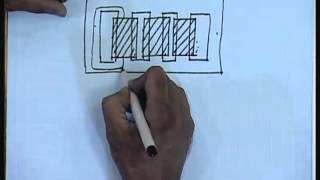
Electrical Machines-I by Prof. Debaprasad Kastha, Department of Electrical Engineering, IIT Kharagpur. For more details on NPTEL visit http://nptel.iitm.ac.in

Electrical Machines-I by Prof. Debaprasad Kastha, Department of Electrical Engineering, IIT Kharagpur. For more details on NPTEL visit http://nptel.iitm.ac.in

Electrical Machines-I by Prof. Debaprasad Kastha, Department of Electrical Engineering, IIT Kharagpur. For more details on NPTEL visit http://nptel.iitm.ac.in
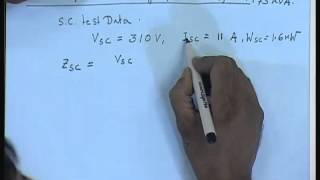
Electrical Machines-I by Prof. Debaprasad Kastha, Department of Electrical Engineering, IIT Kharagpur. For more details on NPTEL visit http://nptel.iitm.ac.in
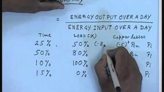
Electrical Machines-I by Prof. Debaprasad Kastha, Department of Electrical Engineering, IIT Kharagpur. For more details on NPTEL visit http://nptel.iitm.ac.in

Electrical Machines-I by Prof. Debaprasad Kastha, Department of Electrical Engineering, IIT Kharagpur. For more details on NPTEL visit http://nptel.iitm.ac.in
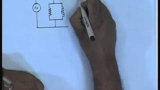
Electrical Machines-I by Prof. Debaprasad Kastha, Department of Electrical Engineering, IIT Kharagpur. For more details on NPTEL visit http://nptel.iitm.ac.in

Electrical Machines-I by Prof. Debaprasad Kastha, Department of Electrical Engineering, IIT Kharagpur. For more details on NPTEL visit http://nptel.iitm.ac.in